AD797
ABSO LUTE MAXIMUM RATINGS 1
3T he AD797’s inputs are protected by back-to-back diodes. T o achieve low noise,
internal current limiting resistors are not incorporated into the design of this
amplifier. If the differential input voltage exceeds ±0.7 V, the input current should
be limited to less than 25 mA by series protection resistors. Note, however, that this
will degrade the low noise performance of the device.
Supply Voltage . . . . . . . . . . . . . . . . . . . . . . . . . . . . . . . . ±18 V
Internal Power Dissipation @ +25°C2
Input Voltage . . . . . . . . . . . . . . . . . . . . . . . . . . . . . . . . . . . ±VS
Differential Input Voltage3 . . . . . . . . . . . . . . . . . . . . . . ±0.7 V
Output Short Circuit Duration . . . . . . . Indefinite Within max
Internal Power Dissipation
Storage Temperature Range (Cerdip) . . . . . . –65°C to +150°C
Storage Temperature Range (N, R Suffix) . . –65°C to +125°C
Operating T emperature Range
AD797A/B . . . . . . . . . . . . . . . . . . . . . . . . . –40°C to +85°C
AD797S . . . . . . . . . . . . . . . . . . . . . . . . . . –55°C to +125°C
Lead T emperature Range (Soldering 60 sec) . . . . . . . +300°C
ESD SUSCEP TIBILITY
ESD (electrostatic discharge) sensitive device. Electrostatic
charges as high as 4000 volts, which readily accumulate on the
human body and on test equipment, can discharge without
detection. Although the AD797 features proprietary ESD pro-
tection circuitry, permanent damage may still occur on these
devices if they are subjected to high energy electrostatic dis-
charges. T herefore, proper ESD precautions are recommended
to avoid any performance degradation or loss of functionality.
NOT ES
1Stresses above those listed under “Absolute Maximum Ratings” may cause
permanent damage to the device. T his is a stress rating only, and functional
operation of the device at these or any other conditions above those indicated in the
operational section of this specification is not implied. Exposure to absolute
maximum rating conditions for extended periods may affect device reliability.
2Internal Power Dissipation:
O RD ERING GUID E
Tem perature
Range
P ackage
D escription
P ackage
O ption
Model
8-Pin SOIC = 0.9 Watts (T A–25°C)/θJA
8-Pin Plastic DIP and Cerdip = 1.3 Watts – (T A–25°C)/θJA
T hermal Characteristics
8-Pin Plastic DIP Package: θJA = 95°C/W
8-Pin Cerdip Package: θJA = 110°C/W
AD797AN
AD797BN
AD797BR
AD797BR-REEL
AD797BR-REEL7
AD797AR
AD797AR-REEL
AD797AR-REEL7
–40°C to +85°C
–40°C to +85°C
–40°C to +85°C
–40°C to +85°C
–40°C to +85°C
–40°C to +85°C
–40°C to +85°C
–40°C to +85°C
8-Pin Plastic DIP
8-Pin Plastic DIP
8-Pin Plastic SOIC
8-Pin Plastic SOIC
8-Pin Plastic SOIC
8-Pin Plastic SOIC
8-Pin Plastic SOIC
8-Pin Plastic SOIC
8-Pin Cerdip
N-8
N-8
SO-8
SO-8
SO-8
SO-8
SO-8
SO-8
Q-8
8-Pin Small Outline Package: θJA = 155°C/W
5962-9313301MPA –55°C to +125°C
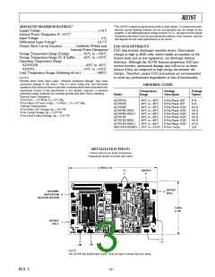
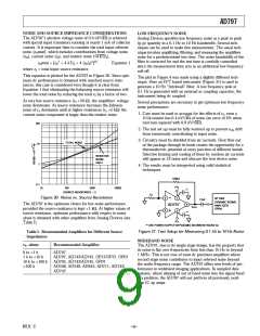
METALIZATIO N P H O TO
Contact factory for latest dimensions.
D imensions shown in inches and (mm).
NOT E
T he AD797 has double layer metal. Only one layer is shown here for clarity.
REV. C
–3–

 ETC [ ETC ]