AD797
Ultr asound/Sonar Im aging P r eam p
–30
–40
–50
–60
–70
–80
100
80
60
40
20
0
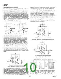
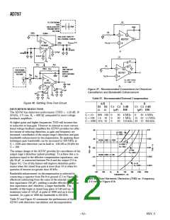
T he AD600 variable gain amplifier provides the time controlled
gain (T CG) function necessary for very wide dynamic range so-
nar and low frequency ultrasound applications. Under some cir-
cumstances, it is necessary to buffer the input of the AD600 to
preserve its low noise performance. T o optimize dynamic range
this buffer should have at most 6 dB of gain. T he combination
of low noise and low gain is difficult to achieve. T he input
buffer circuit shown in Figure 47 provides 1 nV/√Hz noise per-
formance at a gain of two (dc to 1 MHz) by using 26.1 Ω resistors
in its feedback path. Distortion is only –50 dBc @ 1 MHz at a
2 volt p-p output level and drops rapidly to better than
–70 dBc at an output level of 200 mV p-p.
V
OUT
NOISE
26.1Ω
100
1k
10k
100k
1M
10M
100M
FREQUENCY – Hz
**
+V
S
Figure 49. Total Integrated Voltage Noise & VOUT of
Am orphous Detector Pream p
**
26.1
Ω
7
AD797
4
2
3
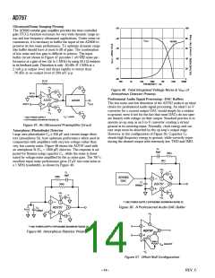
P r ofessional Audio Signal P r ocessing—D AC Buffer s
6
AD600
V
T he low noise and low distortion of the AD797 make it an ideal
choice for professional audio signal processing. An ideal I-to-V
converter for a current output DAC would simply be a resistor
to ground, were it not for the fact that most DACs do not oper-
ate linearly with voltage on their output. Standard practice is to
operate an op amp as an I-to-V converter creating a virtual
ground at its inverting input. Normally, clock energy and cur-
rent steps must be absorbed by the op amp’s output stage.
However, in the configuration of Figure 50, Capacitor CF
shunts high frequency energy to ground, while correctly repro-
ducing the desired output with extremely low T HD and IMD.
INPUT
OUT
**
**
–V
S
V
= ±6Vdc
* USE POWER SUPPLY
** BYPASSING SHOWN IN FIGURE 32.
S
Figure 47. An Ultrasound Pream plifier Circuit
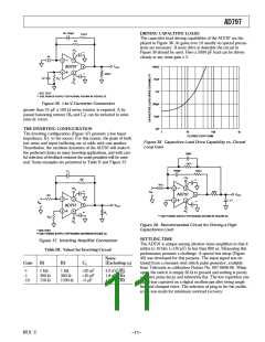
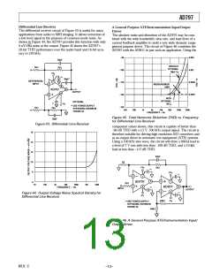
Am or phous (P hotodiode) D etector
Large area photodiodes CS ≥ 500 pF and certain image detec-
tors (amorphous Si), have optimum performance when used in
conjunction with amplifiers with very low voltage rather than
very low current noise. Figure 48 shows the AD797 used with
an amorphous Si (CS = 1000 pF) detector. T he response is ad-
justed for flatness using capacitor CL, while the noise is domi-
nated by voltage noise amplified by the ac noise gain. T he 797’s
excellent input noise performance gives 27 µV rms total noise in
a 1 MHz bandwidth, as shown by Figure 49.
C
F
82pF
100Ω
3kΩ
+V
S
**
C
L
50pF
100Ω
AD1862
DAC
2
3
7
C1
2000pF
6
10kΩ
AD797
4
**
+V
S
**
–V
S
** USE POWER SUPPLY BYPASSING SHOWN IN FIGURE 32.
2
3
7
6
Figure 50. A Professional Audio DAC Buffer
C
AD797
S
I
S
1000pF
4
**
–V
S
** USE POWER SUPPLY BYPASSING SHOWN IN FIGURE 32.
Figure 48. Am orphous Detector Pream p
Figure 51. Offset Null Configuration
–14–
REV. C

 ETC [ ETC ]