Proprietary TranSwitch Corporation Information for use Solely by its Customers
L3M
TXC-03452B
DATA SHEET
PLL FILTER CONNECTION TO VCXO
The Desynchronize Block in the receive line side path contains a phase-locked loop (PLL) circuit, which must
be connected to an external voltage-controlled crystal oscillator (VCXO) via an external filter. This arrangement
is designed to meet limits for jitter on the asynchronous line output signal, which is due to signal mapping and
pointer movements.
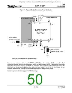
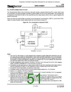
Figure 32 shows the external filter circuit that is recommended for connecting the L3M PLL circuit to the VCXO.
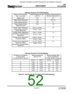
Figure 33 shows the jitter results obtained with the circuit shown in Figure 32.
Figure 32. PLL Connection to External VCXO
R1 806k
C3 3.2
C2 0.01
R2 3M
Inverter
(See Notes 6, 9)
Internal
Op Amp
CTRL
3, D3
U1
AMPINN
5, D4
-
+
AMPOUT
7, E1
AMPINP
6, E2
C1
0.1
R3
1k
GND
13, G2
L3M Device
TXC-03452B
XOSCI
2, D2
X1
VCXO
(See Note 7)
R4
Termination (See Note 5)
Notes:
1. The VCXO PLL filter design is a 2-pole integrator that is designed to supply reliable jitter performance and cap-
ture range with good margins for implementation in high volume production applications. Due to the characteris-
tics of the filter network the signal at AMPOUT will go to a rail in the absence of a DS3/E3 signal in the SONET/
SDH payload. In systems that experience extended Loss of Signal in the TUG-3/STS payload, this characteristic
can cause long capture times, which can exceed 30 seconds.
2. This filter arrangement can be used for TUG-3/DS3, TUG-3/E3, STS-1/DS3 and STS-3/STS-1/DS3 mapping
modes. It provides a bandwidth of 0.3 Hz for DS3 and 0.23 Hz for E3.
3. All resistance (Ω) and capacitance (µF) values must be within 5% and 10%, respectively, of the values shown to
meet the requirements of Figure 33. Two components in series or parallel may be used, where needed.
4. All capacitors must be high quality, non-polarized ceramic types.
5. Termination resistor R4 must be chosen to suit the physical design adopted (e.g., 75 or 50 ohms).
6. Inverter U1 is a Signetics 74HCT04 or equivalent.
7. VCXO X1 is a Fordahl DFV 14-MHR 44.736 MHz V14112 or DFV 14-KHR 34.368 MHz V14111 or equivalent,
depending on the application signal rate.
8. Setting the DIV4 bit (bit 4 in register C7) controls the gain of the phase detector. This bit must be set to 1.
9. Setting the INVCTRL bit (bit 3 in register C7) controls the polarity of the CTRL signal on lead 3 or D3. This bit
must be set to 0 for the circuit shown, which provides the results tabulated in Figure 33. Control bit INVCTRL
allows the use of an external circuit that does not include the inverter U1, if INVCTRL is set to 1.
10. Please contact the TranSwitch Applications Engineering Department if questions arise concerning the PLL filter
design and characteristics.
TXC-03452B-MB
Ed. 6, April 2001
- 51 of 96 -

 ETC [ ETC ]