Proprietary TranSwitch Corporation Information for use Solely by its Customers
L3M
TXC-03452B
DATA SHEET
BOUNDARY SCAN
Introduction
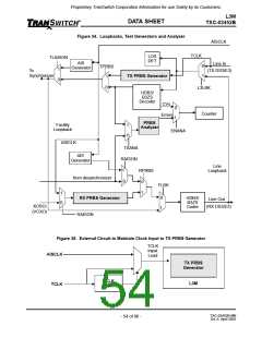
The IEEE 1149.1 standard defines the requirements of a boundary scan architecture that has been specified
by the IEEE Joint Test Action Group (JTAG). Boundary scan is a specialized scan architecture that provides
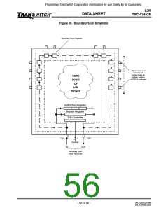
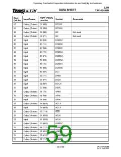
observability and controllability for the interface leads of the device. As shown in Figure 36, one cell of a bound-
ary scan register is assigned to each input or output lead to be observed or tested (bidirectional leads may
have two cells). The boundary scan capability is based on a Test Access Port (TAP) controller, instruction and
bypass registers, and a boundary scan register bordering the input and output leads. The boundary scan test
bus interface consists of four input signals (Test Clock (TCK), Test Mode Select (TMS), Test Data Input (TDI)
and Test Reset (TRS)) and a Test Data Output (TDO) output signal. Boundary scan signal timing is shown in
Figure 29.
The TAP controller receives external control information via a Test Clock (TCK) signal and a Test Mode Select
(TMS) signal, and sends control signals to the internal scan paths. The TAP controller is reset by asserting the
TRS lead low for a minimum of 5 nanoseconds. Detailed information on the operation of this state machine can
be found in the IEEE 1149.1 standard. The serial scan path architecture consists of an instruction register, a
boundary scan register and a bypass register. These three serial registers are connected in parallel between
the Test Data Input (TDI) and Test Data Output (TDO) signals, as shown in Figure 36.
The boundary scan function will be reset and disabled by holding lead TRS low. When boundary scan testing
is not being performed the boundary scan register is transparent, allowing the input and output signals to pass
to and from the L3M device’s internal logic. During boundary scan testing, the boundary scan register may dis-
able the normal flow of input and output signals to allow the device to be controlled and observed via scan
operations.
Boundary Scan Operation
The maximum frequency the L3M device will support for boundary scan is 10 MHz. The timing diagrams for the
boundary scan interface leads are shown in Figure 29.
The instruction register contains three bits. The L3M device performs the following three boundary scan test
instructions:
The EXTEST test instruction (000) provides the ability to test the connectivity of the L3M device to external cir-
cuitry.
The SAMPLE test instruction (010) provides the ability to examine the boundary scan register contents without
interfering with device operation.
The BYPASS test instruction (111) provides the ability to bypass the L3M boundary scan and instruction regis-
ters.
During the Capture - IR state, a fixed value (101) is loaded into the instruction register.
TXC-03452B-MB
Ed. 6, April 2001
- 55 of 96 -

 ETC [ ETC ]