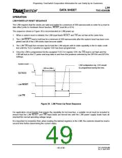
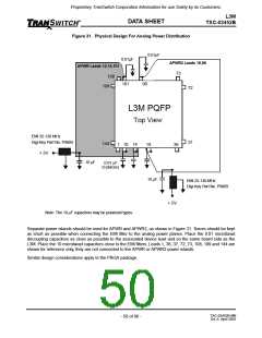
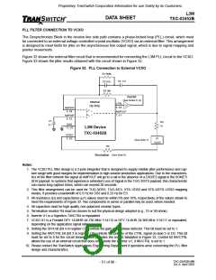
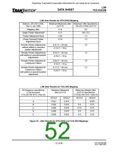
Proprietary TranSwitch Corporation Information for use Solely by its Customers
L3M
TXC-03452B
DATA SHEET
TESTING
Loopbacks
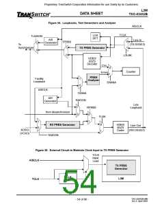
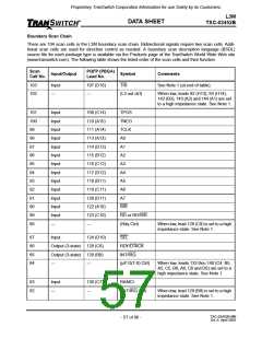
Three loopback capabilities are provided: facility, line and SDH/SONET. Diagrams illustrating the three types of
loopback are provided in the Memory Map Descriptions Section, Address C1, Bits 2-0.
Writing a 1 to control bit FLBK enables facility loopback. Facility loopback and line loopback operations are
shown in Figure 34. When facility loopback is enabled, the internal DS3/E3 transmit signal becomes the inter-
nal receive signal. Either interface may be used, P/N rail or NRZ.
Line loopback is enabled by writing a 1 to control bit L3LBK. The DS3/E3 receive output becomes the transmit
line input. The receive output may be P/N rail or NRZ.
Writing a 1 to control bit SLBK enables a SDH/SONET loopback. SDH/SONET loopback disables the STM-1/
STS-3/STS-1 signal input on the drop bus, and enables the add signals to become the drop bus signals. The
add signals are provided at the add bus.
Test Generators and Analyzers
Two pseudo-random binary sequence (PRBS) test generators are provided, as shown in Figure 34. Each gen-
erator can provide a 215-1 or 223-1 pseudo-random pattern. The test sequence of 223-1 is selected when a 1 is
written into control bit PAT23. When PAT23 is 0, the pattern is 215-1.
The transmit test generator is enabled by writing a 1 to control bit TPRBS. When enabled, the transmit test
generator transmits the pseudo-random pattern in place of transmit NRZ data. The transmit test generator
must have a clock signal provided at the Transmit Line Clock (TCLK) input lead in order to generate a test pat-
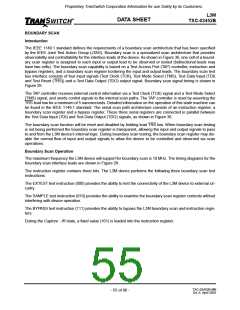
tern. For applications where no transmit line clock is present and the system is required to generate a transmit
PRBS signal, a Loss of Clock detection circuit and a circuit to multiplex the transmit line clock and the AISCLK
should be used externally to maintain a valid clock, as shown in Figure 34.
The receive test generator is enabled by writing a 1 to control bit RPRBS. When enabled, the receive test gen-
erator inserts the pseudo-random test pattern in place of the received desynchronized NRZ data.
The test analyzer is enabled by writing a 1 to control bit ENANA. The test sequence of 223-1 is selected when
a 1 is written into control bit PAT23. Receive NRZ data is analyzed when a 0 is written to control bit TXANA.
When a 1 is written to control bit TXANA, the transmit NRZ data path is monitored. The selection of the test
analyzer disables the decoder CV output to the 16-bit counter. The 16-bit counter now counts received errors
from the test analyzer, when the analyzer is in lock.
TXC-03452B-MB
Ed. 6, April 2001
- 53 of 96 -

 ETC [ ETC ]