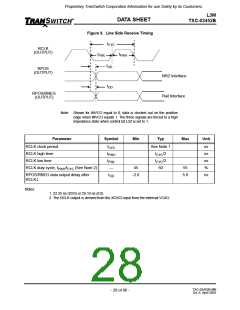
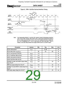
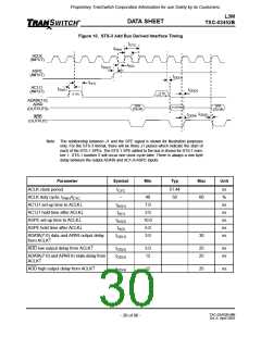
Proprietary TranSwitch Corporation Information for use Solely by its Customers
L3M
TXC-03452B
DATA SHEET
TIMING CHARACTERISTICS
Detailed timing diagrams for the L3M device are illustrated in Figures 7 through 29, with values of the timing
intervals tabulated below the diagrams. All output times are measured with a maximum 25 pF load capaci-
tance. Timing parameters are measured at voltage levels of (VIH + VIL)/2 for input signals or (VOH + VOL)/2 for
output signals.
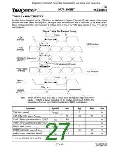
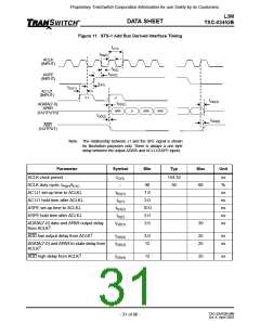
Figure 7. Line Side Transmit Timing
tCYC(1)
TCLK
(INPUT)
tPWH(1)
tSU
tH
NRZ Interface
TPOS
(INPUT)
tSU
tH
TNEG(LOS Indication)
(INPUT)
LOS Indication (NRZ mode)
tSU
tH
TPOS/TNEG
(INPUT)
Rail Interface
tCYC(2)
RNRZC
(OUPUT)
tPWH(2)
tOD
RNRZD
(OUTPUT)
Note: Shown for INVCI equal to 0; data is clocked in on the negative edge when INVCI
equals 1. RNRZD is always clocked out on the positive transitions of RNRZC. The
delay between the input clock TCLK and output clock RNRZC is not specified.
Parameter
TCLK clock period
Symbol
Min
Typ
Max
Unit
tCYC(1)
--
*
ns
%
TCLK duty cycle, tPWH(1)/tCYC(1)
TPOS/TNEG input set-up time to TCLK↑
TPOS/TNEG input hold time after TCLK↑
RNRZC clock period
40
4.0
2.0
50
60
tSU
ns
ns
ns
%
tH
tCYC(2)
--
*
RNRZC duty cycle, tPWH(2)/tCYC(2)
RNRZD output delay after RNRZC↑
40
50
60
tOD
-2.0
5.0
ns
* 22.35 ns (DS3) or 29.10 ns (E3).
TXC-03452B-MB
Ed. 6, April 2001
- 27 of 96 -

 ETC [ ETC ]