Proprietary TranSwitch Corporation Information for use Solely by its Customers
L3M
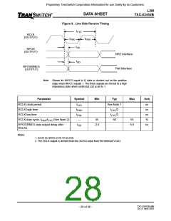
TXC-03452B
DATA SHEET
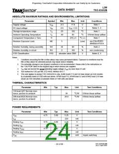
ABSOLUTE MAXIMUM RATINGS AND ENVIRONMENTAL LIMITATIONS
Parameter
Supply voltage
Symbol
Min
Max
Unit
Conditions
Note 1
Notes 1, 3
VDD
VIN
TS
-0.3
-0.5
-55
-40
+7.0
VDD + 0.5
150
V
V
oC
oC
oC x s
DC input voltage
Note 1
Storage temperature range
Ambient Operating Temperature
Component Temperature x Time
Moisture Exposure Level
TA
85
0 ft/min linear airflow
Note 1
TI
270 x 5
per EIA/JEDEC
JESD22-A112-A
ME
5
Level
Relative Humidity, during assembly
Relative Humidity, in-circuit
ESD Classification
RH
RH
30
0
60
%
%
V
Note 2
100
non-condensing
Notes 4, 5
ESD
absolute value 2000
Notes:
1. Conditions exceeding the Min or Max values may cause permanent failure. Exposure to conditions near the
Min or Max values for extended periods may impair device reliability.
2. Pre-assembly storage in non-drypack conditions is not recommended. Please refer to the instructions on
the “CAUTION” label on the drypack bag in which devices are supplied.
3. VIN may not exceed the actual operating supply voltage (VDD) by more than 0.5 volt.
4. Test method for ESD per MIL-STD-883D, Method 3015.7.
5. This note applies to product TXC-03452CIOG only. AGND leads F13 and G4 have shown an ESD sensitiv-
ity at absolute levels of 1500 volts and above. APWR lead F16, APWR lead G1 and APWR2 lead G16 have
shown an ESD sensitivity at absolute levels of 1500 volts and above.
THERMAL CHARACTERISTICS
Parameter
Min
Typ
Max
Unit
Test Conditions
144-lead QFP thermal resis-
tance: junction to ambient
34
oC/W
oC/W
0 ft/min linear airflow
0 ft/min linear airflow
208-lead BGA thermal resis-
tance: junction to ambient
29.0
POWER REQUIREMENTS
Parameter
Min
Typ
Max
Unit
Test Conditions
VDD
4.75
5.00
5.25
220
5.25
30
V
mA
V
IDD
Analog VDD
Analog IDD
Analog VDD2
Analog IDD2
PDD
4.75
4.75
5.00
5.00
mA
V
5.25
1
mA
mW
1320
Inputs switching
TXC-03452B-MB
Ed. 6, April 2001
- 24 of 96 -

 ETC [ ETC ]