Proprietary TranSwitch Corporation Information for use Solely by its Customers
L3M
TXC-03452B
DATA SHEET
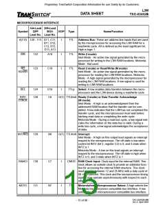
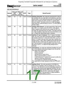
ADD BUS INTERFACE
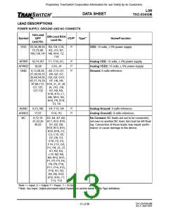
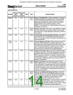
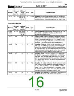
144-Lead 208-Lead
QFP BGA
Lead No. Lead No.
Symbol
I/O/P
Type
Name/Function
APAR
57
O(T) TTL4mA Add Bus Parity Bit: This output bit represents the odd par-
ity calculation for each data byte in the add timing and drop
timing modes. In the external timing mode, the parity calcu-
lation also includes the ASPE and AC1J1 signals which
become outputs. This lead is forced to a high impedance
state when the control bit ADDZ is set to 1, or when ADD is
inactive (high).
T9
ASPE
58
59
I/O(T) TTL4mA Add Bus SPE Indicator: An input signal that is high during
the STM-1 VC-4 period, and STS-3/STS-1 SPE period.
When enabled by the external clock enable (XCLKE) con-
trol lead, this signal becomes an output. This lead is forced
to a high impedance state when the control bit ADDZ is set
to 1, or when the drop timing mode is selected.
R9
AC1J1
I/O(T) TTL4mA Add Bus C1 and J1 Indicator: The C1 pulse is an active
high, one clock cycle wide input timing pulse that identifies
the location of the first C1 time slot in the STM-1 or STS-3
frame. A J1 pulse, also one clock cycle wide, identifies the
location of the J1 byte. When enabled by the external clock
enable (XCLKE) control lead, this signal becomes an out-
put. This lead goes to a high impedance state when control
bit ADDZ is set to 1, or when the drop timing mode is
selected.
N10
ADD
60
O
TTL4mA Add Indicator: An active low signal that identifies the posi-
tion of the data time slots being mapped onto the add bus.
This signal will be high when
T10
- Data is not present
- Reset is present
- Add bus loss of clock occurs
- When control bit ADDZ is set to 1.
- Until the first two C1 pulses are received in either the
add bus or drop bus timing mode.
This avoids bus contention during start up.
This signal will be a high impedance when the TRI lead is
low.
ACLK
61
I/O TTL4mA Add Bus Clock: This clock operates at 19.44 MHz for
STM-1/STS-3 operation, and at 6.48 MHz for STS-1 bus
operation. The add clock is used for Build Block timing and
for sourcing the add bus byte-wide data (ADATA(7-0)), par-
ity (APAR), and add indicator (ADD). When enabled by the
external clock enable (XCLKE) control lead, this signal
becomes an output. This lead goes to a high impedance
state when control bit ADDZ is set to 1.
R10
TXC-03452B-MB
Ed. 6, April 2001
- 17 of 96 -

 ETC [ ETC ]