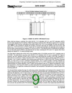
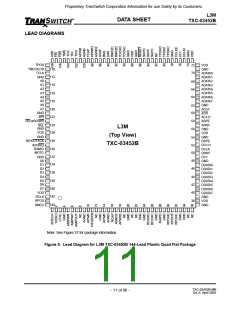
Proprietary TranSwitch Corporation Information for use Solely by its Customers
L3M
TXC-03452B
DATA SHEET
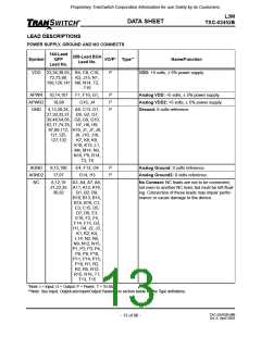
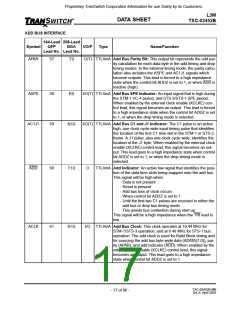
LEAD DESCRIPTIONS
POWER SUPPLY, GROUND AND NO CONNECTS
144-Lead
QFP
Lead No.
208-Lead BGA
Symbol
I/O/P* Type**
Name/Function
Lead No.
VDD 23,34,38,55, B4, C9, C16,
72,73,88, K3, J15, N1,
P
VDD: +5 volts, ± 5% power supply.
108,126,141 N8, N14, T2,
T16
APWR
APWR2
GND
10,14,101
18,98
F1, F16, G1,
G16, J4
P
P
P
Analog VDD: +5 volts, ± 5% power supply.
Analog VDD2: +5 volts, ± 5% power supply.
Ground: 0 volts reference.
4,13,20,24, A9, C13, D1,
27,29,33,37, D8, G2, G7,
39,48,54,56, G8, G9, G10,
62,71,74,78, H7, H8, H9,
87,89,112, H10, J1, J7, J8,
121,125,
127,132
J9, J10, J16,
K7, K8, K9,
K10, K13, L1,
M4, M14, N3,
N16, P9, R14,
T3, T8
AGND
AGND2
NC
9,15,100
17,97
E4, F13, G4
G14, H3
P
P
Analog Ground: 0 volts reference.
Analog Ground2: 0 volts reference.
8,12,19
21,22,35 A11, A12, A16,
36,82
A3, A4, A7, A8,
No Connect: NC leads are not to be connected,
not even to another NC lead, but must be left float-
ing. Connection of these leads may impair perfor-
mance or cause damage to the device.
B1, B2, B9,
B10, B13, B14,
B15, B16, C1,
C3, C15, D5,
D7, D9, E3,
E16, F2, F4,
F14, F15, G3,
H1, H4, J2, J3,
K1, K2, K4,
L14, N2, N5,
N9, N12, N15,
P1, P2, P3, P4,
P6, P8, P10,
P11, P14, P15,
P16, R1, R2,
R3, R5, R12,
R15, R16, T1,
T13, T15
*Note: I = Input; O = Output; P = Power; T = Tri-State
**Note: See Input, Output and Input/Output Parameters section below for the Type definitions.
TXC-03452B-MB
Ed. 6, April 2001
- 13 of 96 -

 ETC [ ETC ]