Proprietary TranSwitch Corporation Information for use Solely by its Customers
L3M
TXC-03452B
DATA SHEET
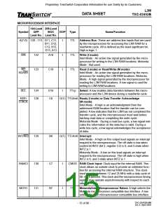
MICROPROCESSOR INTERFACE
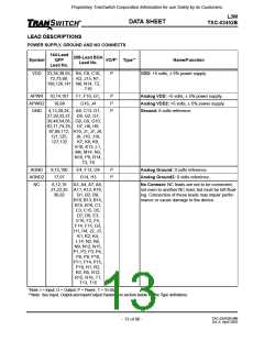
144-Lead 208-Lead
Symbol
QFP
BGA
I/O/P Type
Name/Function
Lead No. Lead No.
A(7-0) 120 - 113 D11, C11,
B11, D12,
I
I
I
TTL
TTL
TTL
Address Bus: These are address line inputs that are used
by the microprocessor for accessing the L3M RAM for a
read/write cycle. A0 is defined as the least significant bit.
High is logic 1.
C12, B12,
D13, A13
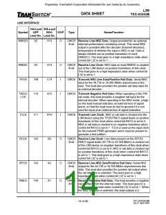
WR
122
123
A10
Write (I mode):
Intel Mode - An active low signal generated by the micro-
processor for writing to the L3M RAM locations. Motorola
Mode - Not used.
RD
C10
Read (I mode) or Read/Write (M mode):
RD/WR
Intel Mode - An active low signal generated by the micro-
processor for reading the L3M RAM locations. Motorola
Mode - A high signal generated by the microprocessor for
reading the L3M RAM locations. A low signal is used for
writing to L3M RAM locations.
SEL
124
128
D10
C8
I
TTLp Select: A low enables data transfers between the micro-
processor and the L3M device during a read/write cycle.
RDY/
DTACK
O(T) TTL8mA Ready (I mode) or Data Transfer Acknowledge
(M mode):
Intel Mode - A high is an acknowledgment from the
addressed RAM location that the transfer can be com-
pleted. A low indicates that the L3M has not completed the
transfer cycle, and the microprocessor must wait before
latching read data or completing the write cycle.
Motorola Mode - During a read bus cycle, a low signal indi-
cates the information on the data bus is valid. During a
write bus cycle, a low signal acknowledges the acceptance
of data.
INT/IRQ
129
B8
O(T) TTL4mA Interrupt:
Intel Mode - A high on this output lead signals an interrupt
request to the microprocessor. The off state is low when
control bit INTZ (bit 2, register C2) is 0, and 3-state when
INTZ is 1.
Motorola Mode - A low on this lead signals an interrupt
request to the microprocessor. The off state is high when
INTZ is 0, and 3-state when INTZ is 1.
RAMCI
MOTO
130
131
C7
B7
I
I
CMOS RAM Clock Input: Clock input for the internal RAM. This
clock allows an outside clock to provide an arbitrator func-
tion for accessing the internal RAM structure. This clock
must operate between 12 and 25 MHz with a duty cycle of
50 +/- 10 percent. This clock and the microprocessor timing
signals may operate asynchronously with respect to each
other.
TTL
Motorola/Intel Microprocessor Select: A high selects the
Motorola microprocessor compatible bus interface. A low
selects the Intel microprocessor compatible bus interface.
TXC-03452B-MB
Ed. 6, April 2001
- 15 of 96 -

 ETC [ ETC ]