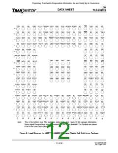
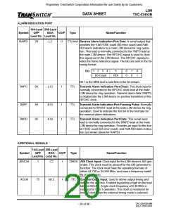
Proprietary TranSwitch Corporation Information for use Solely by its Customers
L3M
TXC-03452B
DATA SHEET
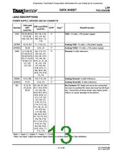
144-Lead 208-Lead
QFP BGA
Lead No. Lead No.
Symbol
I/O/P Type
Name/Function
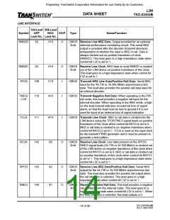
D(7-0) 140 - 133 C4, B5, A5, I/O TTL8mA Data Bus: Bi-directional data lines used for transferring
C5, B6, A6,
C6, D6
data between the L3M device and an external microproces-
sor. D0 is defined as the least significant bit. High is logic 1.
DROP BUS INTERFACE
144-Lead 208-Lead
QFP BGA
Symbol
I/O/P Type
Name/Function
Lead No. Lead No.
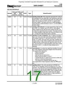
DDATA
(7-0)
40 - 47 R4, T4, N4,
T5, P5, R6,
I
I
TTL
TTL
Drop Data Byte: Byte data that corresponds to the STM-1/
STS-3/STS-1 signal from the drop bus. The first bit
received corresponds to bit 7.
T6, N6
DC1
49
50
R7
Drop C1 Pulse: External positive C1 pulse that may be
provided on this lead instead of in the DC1J1 signal. This
signal is ORed internally with the DC1J1 signal to form a
composite C1J1 signal. If this lead is not used it must be
grounded. This lead is used for special applications.
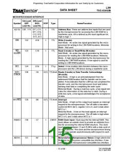
DPAR
T7
I
I
I
I
TTL
TTL
TTL
TTL
Drop Bus Parity Bit: This is an odd parity input for each
data byte, the DSPE signal, and the composite DC1J1
pulses. The status bit BUSERR (bit 5 in registers B0 and
B1) indicates when this input differs from an internally-gen-
erated odd parity for these signals, but no other action is
taken upon occurrence of this drop bus parity error.
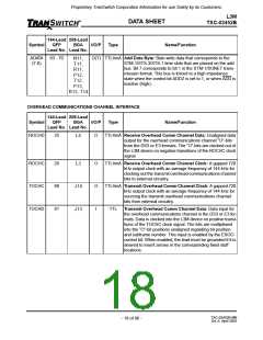
DCLK
DC1J1
DSPE
51
52
53
P7
N7
R8
Drop Bus Clock: This clock operates at 19.44 MHz for
STM-1/STS-3 operation, and at 6.48 MHz for STS-1 bus
operation. Drop bus byte-wide data (DDATA7-0), parity
(DPAR), payload indicator (DSPE), and C1/J1 (DC1J1 and
DC1) are clocked into the L3M device on negative transi-
tions of this clock.
Drop Bus C1 and J1 Indicator: The C1 pulse is an active
high, one clock cycle wide timing pulse that indicates the
location of the first C1 time slot in the STM-1 or STS-3
frame. If the C1 pulse is not present in this signal, it must
be provided at the DC1 lead. A J1 pulse, also one clock
cycle wide, identifies the location of the J1 byte.
Drop Bus SPE Indicator: A signal that is high during the
STM-1 VC-4, and the STS-3/STS-1 SPE period.
TXC-03452B-MB
Ed. 6, April 2001
- 16 of 96 -

 ETC [ ETC ]