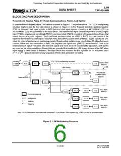
Proprietary TranSwitch Corporation Information for use Solely by its Customers
L3M
TXC-03452B
DATA SHEET
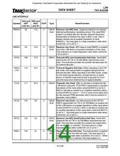
framing pulse (RPOHF), and clock signal (RPOHC). The L3M device also provides a microprocessor-written
location for performing C2 mismatch detection, and unequipped detection based on ANSI and ITU-TSS stan-
dards. The received “O”-bits are available at an external interface and a 2-bit RAM location for these bits is
updated each frame. The “O”-bit interface consists of a data lead (ROCHD) and clock signal (ROCHC). An
alarm indication port is provided for ring operation. The alarm indication port consists of a data lead (RAIPD),
which is used with the POH interface framing pulse (RPOHF) and clock signal (RPOHC). The signal on the
data lead (RAIPD) consists of the FEBE count and a path RDI (FERF) status indication.
The Desynchronize Block removes the effect on the output DS3 or E3 signals of systemic jitter due to signal
mapping and pointer movements. The output has an average frequency equal to the source frequency, and
has jitter characteristics that meet ITU-TSS and ANSI standards. The Desynchronize Block consists of two cir-
cuits, a Pointer Leak circuit and a Phase-Locked Loop circuit. The function of the Pointer Leak circuit is to
absorb the immediate effect of up to eight consecutive pointer movements (any combination of SPE or TUG-3
pointer movements) in either direction, and filter them out in time. A single pointer adjustment is an 8 Unit Inter-
val (UI) phase step. The Pointer Leak circuit turns the phase step into eight 1-UI steps, widely spaced in time,
allowing the Phase-Locked Loop circuit to track. In normal operation, the output is one data bit and one clock
cycle for each input bit. When a negative stuff occurs 8 extra bits are pulled from the signal and absorbed. Fol-
lowing this operation, the normal operation of one bit in for one bit out continues except that one extra bit is
pulled from the FIFO every n frames. In this way, the pointer step is leaked out in 8 x n frames. The value of n
is programmed via the microprocessor.
The Phase-Locked Loop (PLL) circuit of the Desynchronize Block is externally connected to a line-frequency
voltage controlled crystal oscillator (VCXO) via a filter. Details of the external circuit for the PLL are provided in
the Operation section of this Data Sheet under the heading “PLL Filter Connection to VCXO”.
In the Receive direction, the Output Block provides either a positive (RPOS) and negative (RNEG) rail line sig-
nal or a NRZ line signal (RPOS), and a clock signal (RCLK). The HDB3/B3ZS coder operates independently of
the transmitter. For interface flexibility, a control bit is provided for inverting the output clock. The receive data
and clock outputs can be forced to a high impedance state for the purpose of tying two L3M devices together
for ring operation or redundancy. An additional 215-1 or 223-1 pseudo-random test generator is provided. The
Output Block and the Input Block share a 215-1 or 223-1 analyzer that can compare the desynchronizer output
or transmit data against a fixed pattern. An alarm is provided when the analyzer and incoming data are not
synchronous. Errors are counted in the 16-bit coding violation counter. Loopbacks between the Input and Out-
put Blocks facilitate board and network debugging.
All of the control registers and performance counters, and the status and alarm indications, are accessible
through the L3M device’s compatible microprocessor bus interface in the Microprocessor I/O Block. The L3M
device supports both Intel and Motorola microprocessor bus interfaces, with both hardware and software inter-
rupt capability. The Motorola compatible microprocessor interface is selected by placing a high on the MOTO
signal lead.
The Boundary Scan Block provides a mechanism for external access to the input and output leads of the
device, so that they may be observed and tested. The structure and operation of this Block are described in the
Operation section.
TXC-03452B-MB
Ed. 6, April 2001
- 10 of 96 -

 ETC [ ETC ]