3. Data transfer operations
Transmitting: The procedure for transmitting data is as follows.
(1) Set both SO1 and SCK1 to 1 in PMR2 to designate the SO1 and SCK1 pin functions. If
necessary, also designate the SO1 pin as an NMOS open-drain output with bit POF1 in PMR2.
(2) Clear SNC1 in SCR1 to 0, clear or set SNC0 to 0 or 1, and clear MRKON to 0, to select 8-bit
synchronous mode or 16-bit synchronous mode, and select the serial clock with bits CKS3 to
CKS0. When data is written to SCR1 with MRKON in SCR1 cleared to 0, the internal state of
SCI1 is initialized.
(3) Write the transfer data to SDRL/SDRU.
8-bit transfer mode: SDRL
16-bit transfer mode: Upper byte to SDRU, lower byte to SDRL
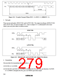
(4) When STF is set to 1 in SCSR1, SCI1 starts operating and transmit data is output from the SO1
pin.
(5) After transmission is completed, IRRS1 is set to 1 in IRR1.
When an internal clock is used, the serial clock is output from the SCK1 pin simultaneously with
transmit data output. When transmission ends, the serial clock is not output until the start flag is
next set to 1. During this interval, the SO1 pin continuously outputs the last bit of the previous
data.
When an external clock is used, data is transmitted in synchronization with the clock input from
the SCK1 pin. If the serial clock continues to be input after the end of transmission, this is regarded
as an overrun state, and the ORER flag is set to 1 in SCSR1 (consequently, transmission is not
performed).
While transmission is halted, the output value of the SO1 pin can be changed by means of the SOL
bit in SCSR1.
Receiving: The procedure for receiving data is as follows.
(1) Set both SI1 and SCK1 to 1 in PMR2 to designate the SI1 and SCK1 pin functions.
(2) Clear SNC1 in SCR1 to 0, clear or set SNC0 to 0 or 1, and clear MRKON to 0, to select 8-bit
synchronous mode or 16-bit synchronous mode, and select the serial clock with bits CKS3 to
CKS0. When data is written to SCR1 with MRKON in SCR1 cleared to 0, the internal state of
SCI1 is initialized.
(3) When STF is set to 1 in SCSR1, SCI1 starts operating and receive data is taken in from the SI1
pin.
261

 ETC [ ETC ]