SCK1
SO1
Bit 14
Bit 0
Bit 1
Bit 2
Bit 3
Bit 4
Bit 5
Bit 15
Tail mark
1 frame
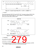
Figure 10-4 Transfer Format (When SNC1 = 0, SNC0 = 1, MRKON = 1)
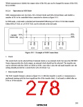
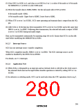
3. Tail mark
There are two tail marks: HOLD TAIL and LATCH TAIL. The output waveforms of HOLD TAIL
and LATCH TAIL are shown in figure 10-5. Time t in figure 10-5 is determined by the serial
clock cycle set by bits CKS2 to CKS0 in SCR1.
HOLD TAIL
SCK1
t
t
t
2t
t
t
t
Bit 14 Bit 15
Bit 0
SO1
LATCH TAIL
SCK1
SO1
t
t
t
2t
t
t
Bit 14 Bit 15
Figure 10-5 HOLD TAIL and LATCH TAIL Output Waveforms
4. Transmitting
The procedure for transmitting data is as follows.
(1) Set SOL to 1 in SCSR1.
(2) Set both SO1 and SCK1 to 1 in PMR2 to designate the SO1 and SCK1 pin functions. Set POF1
to 1 in PMR2 to designate the SO1 pin as an NMOS open-drain output.
264

 ETC [ ETC ]