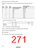
Bit 7: SCI1 module standby mode control (S1CKSTP)
Bit 7 controls setting and clearing of module standby mode for SCI1.
Bit 7
S1CKSTP
Description
0
1
SCI1 is set to module standby mode*1
SCI1 module standby mode is cleared
Setting to module standby mode resets SCR1, SCSR1, SDRU and SDRL.
(initial value)
Note:
*
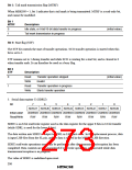
10.2.3
Operation
Either 8-bit or 16-bit transfer data can be selected as the transfer format. An internal clock or
external clock can be selected as the clock source. When an external clock is used, overrun errors
can be detected.
1. Clock
The serial clock can be selected from 8 internal clocks or an external clock. When an internal
clock is selected, the SCK1 pin functions as the clock output pin. When continuous clock output
mode is set (SNC1, SNC0 = 10 in SCR1), the clock selected by bits CKS2 to CKS0 (ø/1024 to
øW/4) is output continuously from the SCK1 pin. When an external clock is selected, the SCK1 pin
functions as the clock input pin.
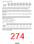
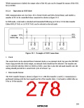
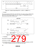
2. Data transfer format
The SCI1 transfer format is shown in figure 10-2. LSB-first transfer is used (i.e. transmission and
reception are performed starting with the least significant bit of the transfer data). Transfer data is
output from one falling edge of the serial clock until the next falling edge. Receive data is latched
at the rising edge of the serial clock.
SCK1
SO1/SI1
Bit 0
Bit 1
Bit 2
Bit 3
Bit 4
Bit 5
Bit 6
Bit 7
Figure 10-2 Transfer Format
260

 ETC [ ETC ]