APEX 20K Programmable Logic Device Family Data Sheet
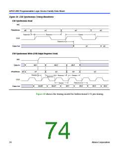
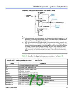
Figure 40. Synchronous Bidirectional Pin External Timing
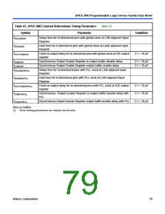
OE Register(1)
PRN
tXZBIDIR
tZXBIDIR
D
Q
Dedicated
Clock
CLRN
tOUTCOBIDIR
Output IOE Register
PRN
Bidirectional Pin
D
Q
tINSUBIDIR
tINHBIDIR
CLRN
IOE Register
Input Register (1)
PRN
(2)
D
Q
CLRN
Notes:
(1) The output enable and input registers are LE registers in the LAB adjacent to a bi-
directional row pin. The output enable register is set with “Output Enable Routing=
Signal-Pin” option in the Quartus II software.
(2) The LAB adjacent input register is set with “Decrease Input Delay to Internal Cells=
Off”. This maintains a zero hold time for lab adjacent registers while giving a fast,
position independent setup time. A faster setup time with zero hold time is possible
by setting “Decrease Input Delay to Internal Cells= ON” and moving the input
register farther away from the bi-directional pin. The exact position where zero
hold occurs with the minimum setup time, varies with device density and speed
grade.
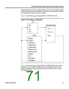
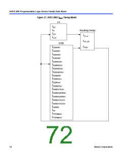
Table 35 describes the fMAX timing parameters shown in Figure 36.
Table 35. APEX 20K fMAX Timing Parameters
Symbol
(Part 1 of 2)
Parameter
t
t
t
t
t
t
t
t
t
t
t
LE register setup time before clock
SU
LE register hold time after clock
LE register clock-to-output delay
LUT delay for data-in
H
CO
LUT
ESBRC
ESB Asynchronous read cycle time
ESB Asynchronous write cycle time
ESBWC
ESB WE setup time before clock when using input register
ESB data setup time before clock when using input register
ESB address setup time before clock when using input registers
ESB clock-to-output delay when using output registers
ESB clock-to-output delay without output registers
ESBWESU
ESBDATASU
ESBADDRSU
ESBDATACO1
ESBDATACO2
Altera Corporation
75

 ETC [ ETC ]