APEX 20K Programmable Logic Device Family Data Sheet
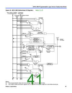
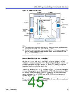
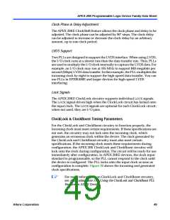
Figure 29. APEX 20KE I/O Banks
I/O Bank 1
I/O Bank 2
I/O Bank 3
(1)
Regular I/O Blocks Support
ꢀ LVTTL
ꢀ LVCMOS
ꢀ 2.5 V
ꢀ 1.8 V
I/O Bank 8
LVDS/LVPECL
Input
Block (2)
ꢀꢀ 3.3 V PCI
ꢀ LVPECL
ꢀ HSTL Class I
ꢀ GTL+
ꢀꢀ SSTL-2 Class I and II
ꢀ SSTL-3 Class I and II
ꢀ CTT
LVDS/LVPECL
Output
Block (2)
I/O Bank 4
(1)
ꢀ AGP
I/O Bank 7
Individual
Power Bus
I/O Bank 6
I/O Bank 5
Notes:
(1) The first two I/ O pins that border the LVDS blocks can only be used for input to
maintain an acceptable noise level on the V plane.
CCIO
(2) If the LVDS input and output blocks are not used for LVDS, they can support all of
the I/ O standards and can be used as input, output, or bidirectional pins with
V
set to 3.3 V, 2.5 V, or 1.8 V.
CCIO
Power Sequencing & Hot Socketing
Because APEX 20K and APEX 20KE devices can be used in a mixed-
voltage environment, they have been designed specifically to tolerate any
possible power-up sequence. Therefore, the VCCIO and VCCINT power
supplies may be powered in any order.
Signals can be driven into APEX 20K devices before and during power-up
without damaging the device. In addition, APEX 20K devices do not drive
out during power-up. Once operating conditions are reached and the
device is configured, APEX 20K and APEX 20KE devices operate as
specified by the user.
Under hot socketing conditions, APEX 20KE devices will not sustain any
damage, but the I/ O pins will drive out.
Altera Corporation
45

 ETC [ ETC ]