APEX 20K Programmable Logic Device Family Data Sheet
Advanced I/O Standard Support
APEX 20KE IOEs support the following I/ O standards: LVTTL,
LVCMOS, 1.8-V I/ O, 2.5-V I/ O, 3.3-V PCI, PCI-X, 3.3-V AGP, LVDS,
LVPECL, GTL+, CTT, HSTL Class I, SSTL-3 Class I and II, and SSTL-2
Class I and II.
For more information on I/ O standards supported by APEX 20KE
devices, see Application Note 117 (Using Selectable I/O Standards in Altera
Devices).
f
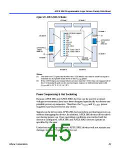
The APEX 20KE device contains eight I/ O banks. In QFP packages, the
banks are linked to form four I/ O banks. The I/ O banks directly support
all standards except LVDS and LVPECL. All I/ O banks can support LVDS
and LVPECL with the addition of external resistors. In addition, one block
within a bank contains circuitry to support high-speed True-LVDS and
LVPECL inputs, and another block within a particular bank supports
high-speed True-LVDS and LVPECL outputs. The LVDS blocks support
all of the I/ O standards. Each I/ O bank has its own VCCIOpins. A single
device can support 1.8-V, 2.5-V, and 3.3-V interfaces; each bank can
support a different standard independently. Each bank can also use a
separate VREF level so that each bank can support any of the terminated
standards (such as SSTL-3) independently. Within a bank, any one of the
terminated standards can be supported. EP20K300E and larger
APEX 20KE devices support the LVDS interface for data pins (smaller
devices support LVDS clock pins, but not data pins). All EP20K300E and
larger devices support the LVDS interface for data pins up to 155 Mbit per
channel; EP20K400E devices and larger with an X-suffix on the ordering
code add a serializer/ deserializer circuit and PLL for higher-speed
support.
Each bank can support multiple standards with the same VCCIOfor
output pins. Each bank can support one voltage-referenced I/ O standard,
but it can support multiple I/ O standards with the same VCCIOvoltage
level. For example, when VCCIO is 3.3 V, a bank can support LVTTL,
LVCMOS, 3.3-V PCI, and SSTL-3 for inputs and outputs.
When the LVDS banks are not used as LVDS I/ O banks, they support all
of the other I/ O standards. Figure 29 shows the arrangement of the
APEX 20KE I/ O banks.
44
Altera Corporation

 ETC [ ETC ]