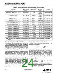
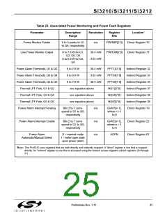
Si3210/Si3211/Si3212
and average input currents can become large with small Monitor pins detect an overload condition, the dc-dc
input voltages. Consider this when selecting the converter interrupts its conversion cycles regardless of
appropriate input voltage and power rating for the V
power supply (number of REN supported).
the register settings to prevent component damage.
These inputs should be calibrated by writing the DCCAL
bit (bit 7) of the dc-dc Converter Switching Delay
register, direct Register 93, after the dc-dc converter
has been turned on.
DC
For this solution, an n-channel power MOSFET (M1)
switches the current flow through a power transformer
T1. T1 is specified in Application Note 45 (AN45), and
includes several taps on the primary side to facilitate a Because the Si3210 dynamically regulates its own
wide range of input voltages. The Si3210M version of battery supply voltage using the dc-dc converter
the Si3210 must be used for the application circuit controller, the battery voltage (V
) is offset from the
BAT
depicted in Figure 9 because the DCFF pin is used to negative-most terminal by a programmable voltage
drive M1 directly and therefore must be the same (V ) to allow voltage headroom for carrying audio
OV
polarity as DCDRV. DCDRV is not used in this circuit signals.
option; connecting DCFF and DCDRV together is not
recommended.
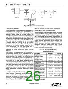
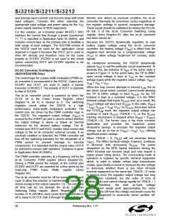
As mentioned previously, the Si3210 dynamically
adjusts V
to suit the particular circuit requirement. To
BAT
illustrate this, the behavior of V
shown in Figure 17. In the active state, the TIP-to-RING
open circuit voltage is kept at V in the constant
voltage region while the regulator output voltage, V
in the active state is
BAT
DC-DC Converter Architecture
(Si3210/Si3210M Only)
OC
The control logic for a pulse width modulated (PWM) dc-
dc converter is incorporated in the Si3210. Output pins,
DCDRV and DCFF, are used to switch a bipolar
transistor or MOSFET. The polarity of DCFF is opposite
to that of DCDRV.
=
BAT
V
+ V + V
.
CM
OC
OV
When the loop current attempts to exceed I , the dc
line driver circuit enters constant current mode allowing
the TIP to RING voltage to track R
LIM
. As the TIP
LOOP
The dc-dc converter circuit is powered on when the
DCOF bit in the Power Down Register (direct
Register 14, bit 4) is cleared to 0. The switching
regulator circuit within the Si3210 is
performance, pulse-width modulation controller. The
control pins are driven by the PWM controller logic in
terminal is kept at a constant voltage, it is the RING
terminal voltage that tracks R and, as a result, the
LOOP
|V | voltage will also track R
. In this state, |V
|
BAT
LOOP
BAT
a
high
= I
R
+ V
+V . As R
decreases below
LIM
LOOP
CM
OV
LOOP
the VOC/I
mark, the regulator output voltage can
LIM
continue to track R
(TRACK = 1), or the R
LOOP
LOOP
the Si3210. The regulated output voltage (V
) is
BAT
tracking mechanism is stopped when |V
| = |V
|
BATL
BAT
sensed by the SVBAT pin and is used to detect whether
the output voltage is above or below an internal
reference for the desired battery voltage. The dc
monitor pins SDCH and SDCL monitor input current and
voltage to the dc-dc converter external circuitry. If an
overload condition is detected, the PWM controller will
turn off the switching transistor for the remainder of a
PWM period to prevent damage to external
components. It is important that the proper value of R18
be selected to ensure safe operation. Guidance is given
in Application Note 45 (AN45).
(TRACK = 0). The former case is the more common
application and provides the maximum power
dissipation savings. In principle, the regulator output
voltage can go as low as |V
significant power savings.
| = V + V , offering
BAT
CM OV
When TRACK = 0, |V
| will not decrease below
BAT
V
. The RING terminal voltage, however, continues
BATL
to decrease with decreasing R
. The power
LOOP
dissipation on the NPN bipolar transistor driving the
RING terminal can become large and may require a
higher power rating device. The non-tracking mode of
operation is required by specific terminal equipment
which, in order to initiate certain data transmission
modes, goes briefly on-hook to measure the line voltage
to determine whether there is any other off-hook
terminal equipment on the same line. TRACK = 0 mode
is desired since the regulator output voltage has long
settling time constants (on the order of tens of
milliseconds) and cannot change rapidly for TRACK = 1
mode. Therefore, the brief on-hook voltage
measurement would yield approximately the same
voltage as the off-hook line voltage and would cause the
terminal equipment to incorrectly sense another off-
hook terminal.
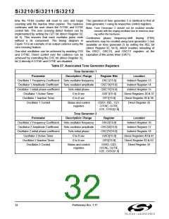
The PWM controller operates at a frequency set by the
dc-dc Converter PWM register (direct Register 92).
During a PWM period the outputs of the control pins
DCDRV and DCFF are asserted for a time given by the
read-only PWM Pulse Width register (direct
Register 94).
The dc-dc converter must be off for some time in each
cycle to allow the inductor or transformer to transfer its
stored energy to the output capacitor, C9. This minimum
off time can be set through the dc-dc Converter
Switching Delay register, (direct Register 93). The
number of 16.384 MHz clock cycles that the controller is
off is equal to DCTOF (bits 0 through 4) plus 4. If the dc
28
Preliminary Rev. 1.11

 ETC [ ETC ]