Si3210/Si3211/Si3212
An internal calibration algorithm corrects for internal and Due to the differences on the driving circuits, there are
external component errors. The calibration is initiated by two different versions of the Si3210. The Si3210
setting the CAL bit in direct Register 96. Upon supports the BJT/inductor circuit option, and the
completion of the calibration cycle, this bit is Si3210M version supports the MOSFET solution. The
automatically reset.
only difference between the two versions is the polarity
of the DCFF pin with respect to the DCDRV pin. For the
Si3210, DCDRV and DCFF are opposite polarity. For
the Si3210M, DCDRV and DCFF are the same polarity.
Table 25 summarizes these differences.
It is recommended that a calibration be executed
following system power-up. Upon release of the chip
reset, the Si3210 will be in the open state. After
powering up the dc-dc converter and allowing it to settle
for time (t
) the calibration can be initiated.
settle
Table 25. Si3210 and Si3210M Differences
Additional calibrations may be performed, but only one
calibration should be necessary as long as the system
remains powered up.
Device
DCFF Signal
Polarity
DCPOL
During calibration, V , V , and V voltages are
RING
Si3210
0
1
= DCDRV
= DCDRV
BAT
TIP
controlled by the calibration engine to provide the
correct external voltage conditions for the algorithm.
Calibration should be performed in the on-hook state.
RING or TIP must not be connected to ground during
the calibration.
Si3210M
Notes:
1. DCFF signal polarity with respect to DCDRV signal.
2. Direct Register 93, bit 5; This is a read-only bit.
Extensive design guidance on each of these circuits can
be obtained from Application Note 45 (AN45) and from
an interactive dc-dc converter design spreadsheet. Both
of these documents are available on the Silicon
Laboratories website (www.silabs.com).
Battery Voltage Generation and Switching
The ProSLIC supports two modes of battery supply
operation. First, the Si3210 integrates a dc-dc converter
controller that dynamically regulates a single output
voltage. This mode eliminates the need to supply large
external battery voltages. Instead, it converts a single
positive input voltage into the real-time battery voltage
needed for any given state according to programmed
linefeed parameters. Second, the Si3211 and Si3212
support switching between high and low battery voltage
supplies, as would a traditional monolithic SLIC.
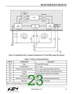
BJT/Inductor Circuit Option Using Si3210
The BJT/Inductor circuit option, as defined in Figure 9,
offers a flexible, low-cost solution. Depending on
selected L1 inductance value and the switching
frequency, the input voltage (V ) can range from 5 V to
DC
30 V. By nature of a dc-dc converter’s operation, peak
and average input currents can become large with small
input voltages. Consider this when selecting the
For single to low channel count applications, the Si3210
proves to be an economical choice, as the dc-dc
converter eliminates the need to design and build high-
voltage power supplies. For higher channel count
applications where centralized battery voltage supply is
economical, or for modular legacy systems where
battery voltage is already available, the Si3211 and
Si3212 are recommended.
appropriate input voltage and power rating for the V
power supply.
DC
For this solution, a PNP power BJT (Q7) switches the
current flow through low ESR inductor L1. The Si3210
uses the DCDRV and DCFF pins to switch Q7 on and
off. DCDRV controls Q7 through NPN BJT Q8. DCFF is
ac coupled to Q7 through capacitor C10 to assist R16 in
turning off Q7. Therefore, DCFF must have opposite
polarity to DCDRV, and the Si3210 (not Si3210M) must
be used.
DC-DC Converter General Description
(Si3210/Si3210M Only)
The dc-dc converter dynamically generates the large
negative voltages required to operate the linefeed
interface. The Si3210 acts as the controller for a buck-
boost dc-dc converter that converts a positive dc
voltage into the desired negative battery voltage. In
addition to eliminating external power supplies, this
allows the Si3210 to dynamically control the battery
voltage to the minimum required for any given mode of
operation.
MOSFET/Transformer Circuit Option Using Si3210M
The MOSFET/transformer circuit option, as defined in
Figure 11, offers higher power efficiencies across a
larger input voltage range. Depending on the
transformers primary inductor value and the switching
frequency, the input voltage (V ) can range from 3.3 V
DC
to 35 V. Therefore, it is possible to power the entire
ProSLIC solution from a single 3.3 V or 5 V power
supply. By nature of a dc-dc converter’s operation, peak
Two different dc-dc circuit options are offered: a BJT/
inductor version and a MOSFET/transformer version.
Preliminary Rev. 1.11
27

 ETC [ ETC ]