Si3035
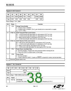
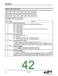
Register 14. Daisy-Chain Control
Bit
D7
D6
D5
D4
D3
D2
D1
D0
Name NSLV2 NSLV1 NSLV0 SSEL1 SSEL0 FSD RPOL DCE
Type
R/W
R/W
R/W
R/W
R/W
R/W R/W R/W
Reset settings = 0000_0010 (serial mode 0, 1)
Reset settings = 0011_1111 (serial mode 2)
Bit
Name
Function
7:5 NSLV[2:0] Number of Slave Devices.
000 = 0 slaves. Simply redefines the FC/RGDT and RGDT/FSD pins.
001 = 1 slave device.
010 = 2 slave devices.
011 = 3 slave devices.
100 = 4 slave devices. (For four or more slave devices, the FSD bit MUST be set.)
101 = 5 slave devices.
110 = 6 slave devices.
111 = 7 slave devices.
4:3 SSEL[1:0] Slave Device Select.
00 = 16-bit SDO receive data.
01 = Reserved.
10 = 15-bit SDO receive data. LSB = 1 for the Si3035 device.
11 = 15-bit SDO receive data. LSB = 0 for the Si3035 device.
2
FSD
Delayed Frame Sync Control.
0 = Sets the number of SCLK periods between frame syncs to 32.
1 = Sets the number of SCLK periods between frame syncs to 16. This bit MUST be set when
Si3035 devices are slaves. For the master Si3035, only serial mode 1 is allowed in this case.
1
0
RPOL
DCE
Ring Detect Polarity.
0 = The FC/RGDT pin (operating as ring detect) is active low.
1 = The FC/RGDT pin (operating as ring detect) is active high.
Daisy-Chain Enable.
0 = Daisy chaining disabled.
1 = Enables the Si3035 to operate with slave devices on the same serial bus. The FC/RGDT
signal (pin 7) becomes the ring detect output and the RDGT/FSD signal (pin 15) becomes the
delayed frame sync signal. Note that ALL other bits in this register are ignored if DCE = 0.
42
Rev. 1.2

 ETC [ ETC ]