Si3035
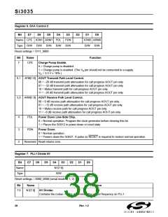
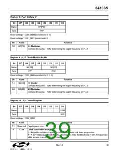
Register 8. PLL1 Multiply M1
Bit
D7
D6
D5
D4
M1[7:0]
R/W
D3
D2
D1
D0
Name
Type
Reset settings = 0000_0000 (serial mode 0, 1)
Reset settings = 0001_0011 (serial mode 2)
Bit
Name
Function
7:0
M1[7:0]
M1 Multiplier.
Contains the (value – 1) for determining the output frequency on PLL1
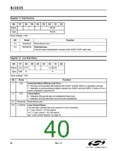
Register 9. PLL2 Divide/Multiply N2/M2
Bit
D7
D6
N2[3:0]
R/W
D5
D4
D3
D2
M2[3:0]
R/W
D1
D0
Name
Type
Reset settings = 0000_0000 (serial mode 0, 1, 2)
Bit
Name
Function
7:4
N2[3:0]
N2 Divider.
Contains the (value – 1) for determining the output frequency on PLL2.
3:0
M2[3:0]
M2 Multiplier.
Contains the (value – 1) for determining the output frequency on PLL2.
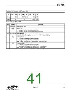
Register 10. PLL Control Register
Bit
D7
D6
D5
D4
D3
D2
D1
D0
Name
Type
CGM
R/W
Reset settings = 0000_0000
Bit
7:1
0
Name
Reserved Read returns zero.
CGM Clock Generation Mode.
0 = No additional ratio is applied to the PLL and faster lock times are possible.
Function
1 = A 25/16 ratio is applied to the PLL allowing for a more flexible choice of MCLK frequencies
while slowing down the PLL lock time.
Rev. 1.2
39

 ETC [ ETC ]