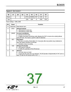
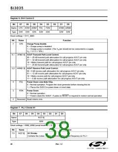
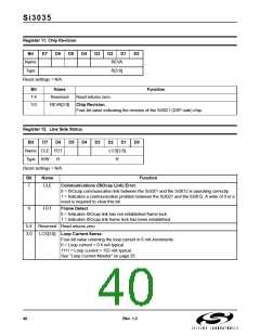
Si3035
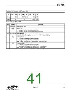
Register 13. Transmit and Receive Gain
Bit
D7
D6
CBID
R
D5
D4
D3
D2
D1
D0
Name
Type
REVB[3:0]
R
ARX ATX
R/W R/W
Reset settings = 0000_0000
Bit
7
Name
Reserved Read returns zero.
CBID Chip B ID.
Function
6
0 = Indicates the line side is domestic only.
1 = Indicates the line side has international support.
5:2 REVB[3:0] Chip Revision.
Four-bit value indicating the revision of the Si3012 (line-side) chip.
Receive Gain.
1
ARX
0 = 0 dB gain is applied to the receive path.
1 = 6 dB gain is applied to the receive path.
Note: This bit should be zero if using Register 15 to control gain.
0
ATX
Transmit Gain.
0 = 0 dB gain is applied to the receive path.
1 = –3 dB gain (attenuation) is applied to the transmit path.
Note: This bit should be 0 if using Register 15 to control gain.
Rev. 1.2
41

 ETC [ ETC ]