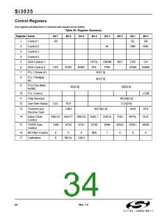
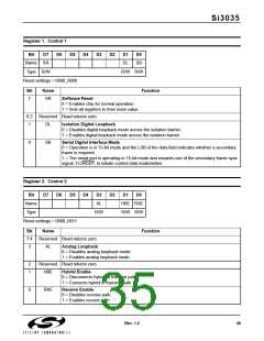
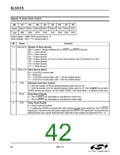
Si3035
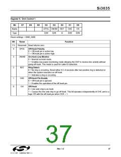
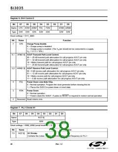
Register 6. DAA Control 2
Bit
Name CPE ATM1 ARM1 PDL PDN
Type R/W R/W R/W R/W R/W
Reset settings = 0111_0000
D7
D6
D5
D4
D3
D2
D1
ATM0 ARM0
R/W R/W
D0
Bit
Name
Function
7
CPE
Charge Pump Enable.
0 = Charge pump is disabled.
1 = Charge pump is enabled. (The VA pin should not be connected to a supply.
VD = 3.3 V ± 10%.)
6,1 ATM[1:0] AOUT Transmit Path Level Control.
00 = –20 dB transmit path attenuation for call progress AOUT pin only.
01 = –32 dB transmit path attenuation for call progress AOUT pin only.
10 = Mutes transmit path for call progress AOUT pin only.
11 = –26 dB transmit path attenuation for call progress AOUT pin only.
5,0 ARM[1:0] AOUT Receive Path Level Control.
00 = 0 dB receive path attenuation for call progress AOUT pin only.
01 = –12 dB receive path attenuation for call progress AOUT pin only.
10 = Mutes receive path for call progress AOUT pin only.
11 = –6 dB receive path attenuation for call progress AOUT pin only.
4
3
2
PDL
PDN
Power Down Line-Side Chip.
0 = Normal operation. Program the clock generator before clearing this bit.
1 = Places the Si3012 in power down or reset state.
Power Down.
0 = Normal operation.
1 = Powers down the Si3021. A pulse on RESET is required to restore normal operation.
Reserved Read returns zero.
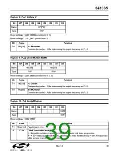
Register 7. PLL1 Divide N1
Bit
D7
D6
D5
D4
N1[7:0]
R/W
D3
D2
D1
D0
Name
Type
Reset settings = 0000_0000 (serial mode 0, 1, 2)
Bit
Name
Function
7:0
N1[7:0]
N1 Divider.
Contains the (value – 1) for determining the output frequency on PLL1.
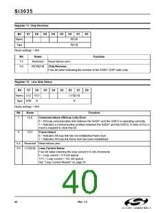
38
Rev. 1.2

 ETC [ ETC ]