Si3035
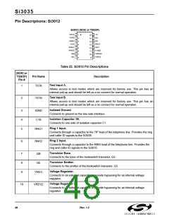
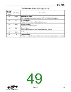
Pin Descriptions: Si3021
Si3021 (SOIC)
Si3021 (TSSOP)
MCLK
FSYNC
SCLK
OFHK
RGDT/FSD
M0
1
1
2
3
4
5
6
7
8
SDO
SDI
VD
16
16
15
14
13
12
11
10
9
2
SCLK
FSYNC
MCLK
OFHK
RGDT/FSD
M0
15
FC/RGDT
RESET
AOUT
M1
3
4
5
6
7
8
14
13
12
11
10
9
VD
VA
SDO
GND
C1A
SDI
FC/RGDT
RESET
M1
C1A
AOUT
GND
VA
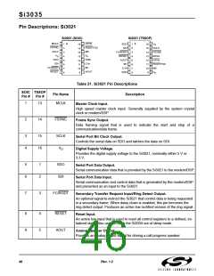
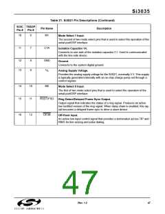
Table 21. Si3021 Pin Descriptions
Description
SOIC TSSOP
Pin Name
Pin #
Pin #
1
13
MCLK
Master Clock Input.
High speed master clock input. Generally supplied by the system crystal
clock or modem/DSP.
2
14
FSYNC
Frame Sync Output.
Data framing signal that is used to indicate the start and stop of a
communication/data frame.
3
4
15
16
SCLK
VD
Serial Port Bit Clock Output.
Controls the serial data on SDO and latches the data on SDI.
Digital Supply Voltage.
Provides the digital supply voltage to the Si3021, nominally either 5 V or
3.3 V.
5
6
1
2
SDO
SDI
Serial Port Data Output.
Serial communication data that is provided by the Si3021 to the modem/DSP.
Serial Port Data Input.
Serial communication and control data that is generated by the modem/DSP
and presented as an input to the Si3021.
7
3
FC/RGDT
Secondary Transfer Request Input/Ring Detect Output.
An optional signal to instruct the Si3021 that control data is being requested
in a secondary frame. When daisy chain is enabled, this pin becomes the
ring detect output. Produces an active low rectified version of the ring signal.
8
9
4
5
RESET
AOUT
Reset Input.
An active low input that is used to reset all control registers to a defined, ini-
tialized state. Also used to bring the Si3034 out of sleep mode.
Analog Speaker Output.
Provides an analog output signal for driving a call progress speaker.
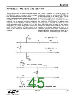
46
Rev. 1.2

 ETC [ ETC ]