Functional Description
Functional Description
4
This chapter describes the 82443BX interfaces on-chip functional units. Section 4.1, “System
Address Map” on page 4-1 provides a system-level address memory map and describes the
memory space controls provided by the 82443BX. This section also describes the I/O address map.
Note that 82443BX register maps are provided in Chapter 3, “Register Description”.
The 82443BX Host-to-PCI Bridge functions are described Host, PCI, and AGP interfaces are
described in Section 4.2, “Host Interface” on page 4-10, Section 4.4, “PCI Interface” on page 4-24,
and Section 4.5, “AGP Interface” on page 4-24.
The DRAM interface including supported DRAM types, organizations, configurations, and register
programming considerations is provided in Section 4.3, “DRAM Interface” on page 4-14. Data
integrity support on the Host bus, PCI bus, and DRAM interface is described in Section 4.6, “Data
Integrity Support” on page 4-25.
System clocking requirements is provided in Section 4.7, “System Clocking” on page 4-28.
The 82443BX has various power management capabilities. Suspend resume, clock control,
SDRAM power down, and SMRAM functions are described in Section 4.8, “Power Management”
on page 4-28. This section also contains information on the 82443BX reset operations.
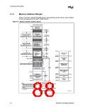
4.1
System Address Map
A Pentium® Pro processor-based system with the Intel® 440BX AGPset supports 4 GB of
addressable memory space and 64 KB + 3 of addressable I/O space. (The Pentium® Pro processor
bus I/O addressability is 64 KB + 3). There is a programmable memory address space under the 1
MB region which is divided into regions which can be individually controlled with programmable
attributes such as Disable, Read/Write, Write Only, or Read Only. Attribute programming is
described in the Register Description section. This section focuses on how the memory space is
partitioned and what these separate memory regions are used for. The I/O address space requires
much simpler mapping and it is explained at the end of this section.
The Pentium Pro processor family supports addressing of memory ranges larger than 4 GB. The
82443BX Host Bridge claims any access over 4 GB by terminating transaction (without forwarding
it to PCI or AGP). Writes are terminated simply by dropping the data and for reads the 82443BX
returns all zeros on the host bus. Note that the 82443BX as a target does not support the PCI Dual
Address Cycle Mechanism (DAC) which allows addressing of >4GB on either the PCI or AGP
interface.
In the following sections, it is assumed that all of the compatibility memory ranges reside on PCI.
The exception to this rule are the VGA ranges which may be mapped to AGP. In the absence of
more specific references, cycle descriptions referencing PCI should be interpreted as PCI, while
cycle descriptions referencing AGP are relate to AGP.
82443BX Host Bridge Datasheet
4-1

 ETC [ ETC ]