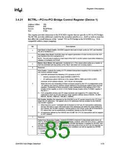
Register Description
3.4.21
BCTRL—PCI-to-PCI Bridge Control Register (Device 1)
Address Offset:
Default:
Access:
3Eh
80h
Read/Write
8 bits
Size
This register provides extensions to the PCICMD1 register that are specific to PCI-to-PCI bridges.
The BCTRL provides additional control for the secondary interface (i.e., AGP) as well as some bits
that affect the overall behavior of the “virtual” PCI-to-PCI bridge in the 82443BX (e.g., VGA
compatible address ranges mapping).
Bit
Descriptions
Fast Back to Back Enable. 82443BX supports fast back-to-back cycles on AGP, and therefore
this bit is hardwired to 1.
7
Secondary Bus Reset: 82443BX does not support generation of reset via this bit on the AGP
and therefore this bit is hardwired to 0.
6
NOTE: The only way to perform a hard reset of the AGP is via the system reset either initiated by
software or hardware via PIIX4E.
Master Abort Mode. Not applicable. Hardwired to 0. (This means when acting as a master on
AGP the 82443BX will drop writes on the “floor” and return all 1s during reads.)
5
4
Reserved.
VGA Enable. Controls the routing of CPU-initiated transactions targeting VGA compatible I/O
and memory address ranges.
1 = 82443BX will forward the following CPU accesses to AGP:
•
•
memory accesses in the range 0A0000h to 0BFFFFh
I/O addresses where A[9:0] are in the ranges 3B0h to 3BBh and 3C0h to 3DFh
(inclusive of ISA address aliases - A[15:10] are not decoded)
3
When this bit is set, forwarding of these accesses issued by the CPU is independent of the
I/O address and memory address ranges defined by the previously defined base and limit
registers. Forwarding of these accesses is also independent of the settings of bit 2 (ISA
Enable) of this register or of bit 5 (VGA Palette Snoop Enable) of the PCICMD1 register if
this bit is 1.
0 = VGA compatible memory and I/O range accesses are mapped to PCI unless they are
redirected to AGP via I/O and memory range registers defined above (IOBASE, IOLIMIT,
MBASE, MLIMIT, PMBASE, PMLIMIT). (default)
ISA Enable. Modifies the response by the 82443BX to an I/O access issued by the CPU that
target ISA I/O addresses. This applies only to I/O addresses that are enabled by the IOBASE
and IOLIMIT registers.
1 = When this bit is set to 1 82443BX will not forward to AGP any I/O transactions addressing
the last 768 bytes in each 1KB block even if the addresses are within the range defined by
the IOBASE and IOLIMIT registers. Instead going to AGP these cycles will be forwarded to
PCI where they can be subtractively or positively claimed by the ISA bridge.
2
0 = All addresses defined by the IOBASE and IOLIMIT for CPU I/O transactions will be mapped
to AGP. (default)
1
0
Reserved.
Parity Error Response Enable. Controls 82443BX’s response to data phase parity errors on
AGP. G_PERR# is not implemented by the 82443BX. However, when this bit is set to 1, address
and data parity errors on AGP are reported via SERR# mechanism, if enabled by SERRE1 and
SERRE. If this bit is reset to 0, then address and data parity errors on AGP are not reported via
the 82443BX SERR# signal. Other types of error conditions can still be signaled via SERR#
independent of this bit’s state.
1 = Enable.
0 = Disable.
82443BX Host Bridge Datasheet
3-59

 ETC [ ETC ]