Register Description
The DRAM array can be configured with single or double-sided DIMMs using 2MX8, 4Mx16, or
8Mx8 parts. The array also supports x4 width DRAM components on registered DIMMs. Each
register defines an address range that will cause a particular CS# line (or RAS# in the EDO case) to
be asserted (e.g., if the first DRAM row is minus 8 MB, then accesses within the 0 to 8 MByte
range will cause CSx0#/RASx0# to be asserted). The DRAM Row Boundary (DRB) Registers are
programmed with an 8-bit upper address limit value. This upper address limit is compared to bits
[30:23] of the requested address, for each row, to determine if DRAM is being targeted.
Note: DRAM is selected only if address[31:30] are zero.
Bit
Description
Row Boundary Address. This 8-bit value is compared against address lines A[30:23] to
determine the upper address limit of a particular row (i.e., DRB minus previous DRB = row size).
7:0
NOTE: When PCIRST# assertion occurs during POS/STR, these bits are not reset to ‘01h’.
Row Boundary Address
These 8 bit values represent the upper address limits of the eight rows (i.e., this row minus previous
row = row size). Unpopulated rows have a value equal to the previous row (row size = 0). DRB7
reflects the maximum amount of DRAM in the system. The top of memory is determined by the
value written into DRB7.
Note: The 82443BX supports a maximum of 1 GB of DRAM using registered SDRAM DIMMs. (an
example of this configuration is 4 double-sided registered DIMMs using 16Mx4 parts).
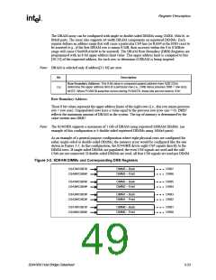
As an example of a general purpose configuration where eight physical rows are configured for
either single-sided or double-sided DIMMs, the memory array would be configured like the one
shown in Figure 3-2. In this configuration, the 82443BX drives eight CS# signals directly to the
DIMM rows. If single-sided DIMMs are populated, the even CS# signals are used and the odd
CS#s are not connected. If double-sided DIMMs are used, all four CS# signals are used per DIMM.
Figure 3-2. SDRAM DIMMs and Corresponding DRB Registers
CSA7#/CSB7#
CSA6#/CSB6#
DIMM3 – Back
DIMM3 – Front
DRB7
DRB6
CSA5#/CSB5#
CSA4#/CSB4#
DIMM2 – Back
DIMM2 – Front
DRB5
DRB4
CSA3#/CSB3#
CSA2#/CSB2#
DIMM1 – Back
DIMM1 – Front
DRB3
DRB2
CSA1#/CSB1#
CSA0#/CSB0#
DIMM0 – Back
DIMM0 – Front
DRB1
DRB0
82443BX Host Bridge Datasheet
3-23

 ETC [ ETC ]