Register Description
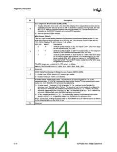
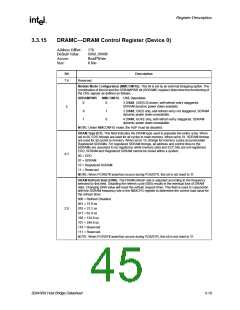
3.3.15
DRAMC—DRAM Control Register (Device 0)
Address Offset:
Default Value:
Access:
57h
00S0_0000b
Read/Write
8 bits
Size:
Bit
Description
7:6
Reserved.
Module Mode Configuration (MMCONFIG). This bit is set by an external strapping option. The
combination of this bit and the SDRAMPWR bit (SDRAMC register) determine the functioning of
the CKE signals as defined as follows:
SDRAMPWR
MMCONFIG CKE Operation
0
0
1
0
3 DIMM, CKE[5:0] driven, self-refresh entry staggered.
SDRAM dynamic power down available.
5
X
1
3 DIMM, CKE0 only, self-refresh entry not staggered. SDRAM
dynamic power down unavailable.
4 DIMM, GCKE only, self-refresh entry staggered. SDRAM
dynamic power down unavailable.
NOTE: Under MMCONFIG mode, the AGP must be disabled.
DRAM Type (DT). This field indicates the DRAM type used to populate the entire array. When
set to 00, EDO timings are used for all cycles to main memory. When set to 01, SDRAM timings
are used for all cycles to memory. When set to 10, timings for memory cycles accommodate
Registered SDRAMs. For registered SDRAM timings, all address and control lines to the
SDRAMs are assumed to be registered, while memory data and ECC bits are not registered.
EDO, SDRAM and Registered SDRAM cannot be mixed within a system.
4:3
00 = EDO
01 = SDRAM
10 = Registered SDRAM
11 = Reserved
NOTE: When PCIRST# assertion occurs during POS/STR, this bit is not reset to ‘0’.
DRAM Refresh Rate (DRR). The DRAM refresh rate is adjusted according to the frequency
selected by this field. Disabling the refresh cycle (000) results in the eventual loss of DRAM
data. Changing DRR value will reset the refresh request timer. This field is used in conjunction
with the SDRAM frequency bits in the NBXCFG register to determine the correct load value for
the refresh timer.
000 = Refresh Disabled
001 = 15.6 us
2:0
010 = 31.2 us
011 = 62.4 us
100 = 124.8 us
101 = 249.6 us
110 = Reserved
111 = Reserved
NOTE: When PCIRST# assertion occurs during POS/STR, this bit is not reset to ‘0’.
82443BX Host Bridge Datasheet
3-19

 ETC [ ETC ]