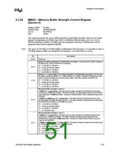
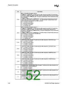
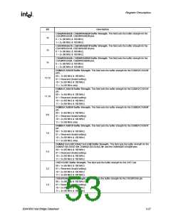
Register Description
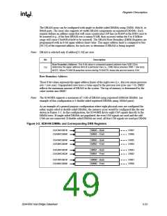
The following 2 examples describe how the DRB Registers are programmed for cases of single-
sided and double-sided DIMMs on a motherboard.
Example #1 Single-sided DIMMs
Assume a total of 16 MB of DRAM are required using single-sided 1MB x 64 DIMMs. In this
configuration, two DIMMs are required.
DRB0 = 01h
DRB1 = 01h
DRB2 = 02h
DRB3 = 02h
DRB4 = 02h
DRB5 = 02h
DRB6 = 02h
DRB7 = 02h
populated (1 DIMM, 8 Mbyte this row)
empty row
populated (1 DIMM, 8 Mbyte this row)
empty row
empty row
empty row
empty row
empty row
Example #2 Mixed Single-/Double-sided DIMMs
As another example, consider a system that is initially shipped with 8 MB of memory using a 1M x
64 DIMM and that rest of the memory array should be upgradable up to a maximum supported
memory of 200 MB. This can be handled by further populating the array with one 16M x 64 single-
sided DIMM (one row) and one 8M x 64 double-sided DIMM (two rows), yielding a total of 200
MB of DRAM. The DRB Registers are programmed as follows:
DRB0 = 01h
DRB1 = 01h
DRB2 = 05h
DRB3 = 09h
DRB4 = 19h
DRB5 = 19h
DRB6 = 19h
DRB7 = 19h
populated with 8 MB, 1MB x 64 single-sided DIMM
empty row
populated with 32 MB, 1/2 of 8M x 64 DIMM
populated with 32 MB, the other 1/2 of 8M x 64 DIMM
populated with 128 MB, 16M x 64 single-sided DIMM
empty row
empty row
empty row
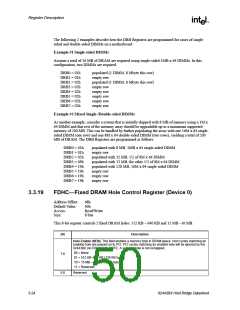
3.3.19
FDHC—Fixed DRAM Hole Control Register (Device 0)
Address Offset:
Default Value:
Access:
68h
00h
Read/Write
8 bits
Size:
This 8-bit register controls 2 fixed DRAM holes: 512 KB – 640 KB and 15 MB –16 MB.
Bit
Description
Hole Enable (HEN). This field enables a memory hole in DRAM space. Host cycles matching an
enabled hole are passed on to PCI. PCI cycles matching an enabled hole will be ignored by the
82443BX (no DEVSEL#). NOTE: A selected hole is not remapped.
00 = None
7:6
5:0
01 = 512 KB–640 KB (128 KB bytes)
10 = 15 MB – 16 MB (1 MB byte)
11 = Reserved
Reserved.
3-24
82443BX Host Bridge Datasheet

 ETC [ ETC ]