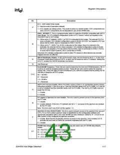
Register Description
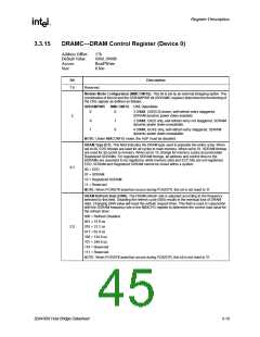
3.3.16
DRAMT—DRAM Timing Register (Device 0)
Address Offset:
Default Value:
Access:
58h
03h
Read/Write
8 bits
Size:
This 8-bit register controls main memory DRAM timings. Refer to the DRAM section for details
regarding the DRAM timings programmed in this register.
Bit
Description
7:2
Reserved.
EDO RASx# Wait State (RWS). When RWS = 1, one additional wait state is inserted before RAS#
is asserted for row misses. This provides one clock of additional MAX[13:0] setup time to RASx#
assertion. This bit does not affect page misses since the MAX[13:0] lines are setup several clocks
in advance of RAS# assertion for page misses.
1
0
0 = 1 tASR
1 = 2 tASR
EDO CASx# Wait State (CWS). When CWS = 1, one additional wait state is inserted before the
assertion of the first CASx# for page hit cycles. This allows one additional clock of MA setup time
to the CASx# for the leadoff page hit cycle. Page miss and row miss timings are not affected by
this bit.
0 = 1 Tasc
1 = 2 Tasc
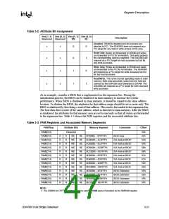
3.3.17
PAM[6:0]—Programmable Attribute Map Registers
(Device 0)
Address Offset:
Default Value:
Attribute:
59h (PAM0) – 5Fh (PAM6)
00h
Read/Write
The 82443BX allows programmable memory attributes on 13 Legacy memory segments of various
sizes in the 640 KB to 1 MB address range. Seven Programmable Attribute Map (PAM) Registers
are used to support these features. Cacheability of these areas is controlled via the MTRR registers
in the Pentium Pro processor. Two bits are used to specify memory attributes for each memory
segment. These bits apply to both host accesses and PCI initiator accesses to the PAM areas. These
attributes are:
RE
Read Enable. When RE = 1, the host read accesses to the corresponding memory segment
are claimed by the 82443BX and directed to main memory. Conversely, when RE = 0, the
host read accesses are directed to PCI.
WE
Write Enable. When WE = 1, the host write accesses to the corresponding memory
segment are claimed by the 82443BX and directed to main memory. Conversely, when WE
= 0, the host write accesses are directed to PCI.
The RE and WE attributes permit a memory segment to be Read Only, Write Only, Read/Write, or
disabled. For example, if a memory segment has RE = 1 and WE = 0, the segment is Read Only.
Each PAM Register controls two regions, typically 16 KB in size. Each of these regions has a 4-bit
field. The four bits that control each region have the same encoding and are defined in Table 3-2.
3-20
82443BX Host Bridge Datasheet

 ETC [ ETC ]