Register Description
3.3.20
MBSC—Memory Buffer Strength Control Register
(Device 0)
Address Offset:
Default Value:
Access:
69–6Eh
000000000000h
Read/Write
48 bits
Size:
This register programs the various DRAM interface signal buffer strengths, based on non-mixed
memory configurations of DRAM type (EDO or SDRAM), DRAM density (x8, x16, or x32),
DRAM technology (16MB or 64 MB), and rows populated. Note that x4 DRAM may only be
supported when used on registered DIMMs.
Note: The choice of 100 MHz or 66 MHz buffer is independent of bus frequency. It is possible to select a
100 MHz memory buffer even though the bus frequency is 66 MHz (and vice versa).
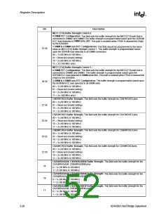
Bit
Description
47:40
Reserved
MAA[13:0], WEA#, SRASA#, SCASA# Buffer Strengths. This field sets the buffer strength for
the MAA[13:0], WEA#, SRASA#, SCASA# pins.
00 = 1x (66 MHz & 100 MHz)
01 = Reserved (Invalid setting)
10 = 2x (66 MHz & 100 MHz)
11 = 3x (66 MHz & 100 MHz)
39:38
37:36
MAB[12:11, 9:0]# & MAB[13,10], WEB#, SRASB#, SCASB# Buffer Strengths. This field sets
the buffer strength for MAB[12:11, 9:0]# & MAB[13,10], WEB#, SRASB#, SCASB# pins. Note
that the address’s MAB# are inverted copies of MAA, with the exception of MAB[13,10].
00 = 1x (66 MHz & 100 MHz)
01 = Reserved (Invalid setting)
10 = 2x (66 MHz & 100 MHz)
11 = 3x (66 MHz & 100 MHz)
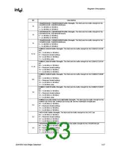
MD [63:0] Buffer Strength Control 2.
4 DIMM FET Configuration: This field sets the buffer strength for the MD[63:0] path that is
connected to DIMM2 and DIMM3. The buffer strength is programmable based on the SDRAM
load in detected in DIMM slots 2&3. This path is enabled when FENA is asserted (High) by the
82443BX.
3 DIMM & 4 DIMM non-FET Configuration: This field should be programmed to the same
value as MD[63:0] Buffer Strength Control 1. This buffer strength is programmable based upon
the SDRAM load detected in all DIMM connectors.
35:34
00 = 1x (66 MHz & 100 MHz)
01 = Reserved (Invalid setting)
10 = 2x (66 MHz & 100 MHz)
11 = 3x (100 MHz only)
MD [63:0] Buffer Strength Control 1.
4 DIMM FET Configuration: This field sets the buffer strength for the MD[63:0] path that is
connected to DIMM0 and DIMM1. The buffer strength is programmable based upon the
SDRAM load in detected in DIMM slots 0&1. This path is enabled when FENA is asserted
(Low) by the 82443BX.
3 DIMM & 4 DIMM non-FET Configurations: The buffer strength is programmable based upon
the SDRAM load detected in all DIMM connectors.
33:32
00 = 1x (66 MHz & 100 MHz)
01 = Reserved (Invalid setting)
10 = 2x (66 MHz & 100 MHz)
11 = 3x (100 MHz only)
82443BX Host Bridge Datasheet
3-25

 ETC [ ETC ]