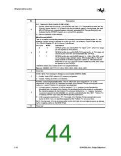
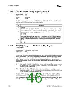
Register Description
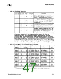
DOS Application Area (00000h–9FFFh)
The DOS area is 640 KB and it is further divided into two parts. The 512 KB area at 0 to 7FFFFh is
always mapped to the main memory controlled by the 82443BX, while the 128 KB address range
from 080000 to 09FFFFh can be mapped to PCI or to main DRAM. By default this range is
mapped to main memory and can be declared as a main memory hole (accesses forwarded to PCI)
via 82443BX’s FDHC configuration register.
Video Buffer Area (A0000h–BFFFFh)
This 128 KB area is not controlled by attribute bits. The host-initiated cycles in this region are
always forwarded to either PCI or AGP unless this range is accessed in SMM mode. Routing of
accesses is controlled by the Legacy VGA control mechanism of the “virtual” PCI-to-PCI bridge
device embedded within the 82443BX.
This area can be programmed as SMM area via the SMRAM register. When used as a SMM space
this range can not be accessed from PCI or AGP.
Expansion Area (C0000h–DFFFFh)
This 128 KB area is divided into eight 16 KB segments which can be assigned with different
attributes via PAM control register as defined by Table 3-3.
Extended System BIOS Area (E0000h–EFFFFh)
This 64 KB area is divided into four 16 KB segments which can be assigned with different
attributes via PAM control register as defined by the Table 3-3.
System BIOS Area (F0000h–FFFFFh)
This area is a single 64 KB segment which can be assigned with different attributes via PAM
control register as defined by the Table 3-3.
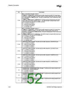
3.3.18
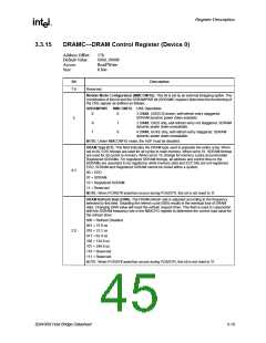
DRB[0:7]—DRAM Row Boundary Registers (Device 0)
Address Offset:
Default Value:
Access:
60h (DRB0) – 67h (DRB7)
01h
Read/Write
Size:
8 bits/register
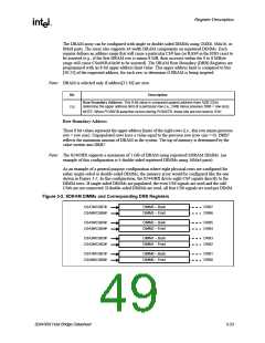
The 82443BX supports 8 physical rows of DRAM. The width of a row is 64 bits. The DRAM Row
Boundary Registers define upper and lower addresses for each DRAM row. Contents of these 8-bit
registers represent the boundary addresses in 8 MB granularity. For example, a value of 01h
indicates 8 MB.
60h
61h
62h
63h
64h
65h
66h
67h
DRB0 = Total memory in row0 (in 8 MB)
DRB1 = Total memory in row0 + row1 (in 8 MB)
DRB2 = Total memory in row0 + row1 + row2 (in 8 MB)
DRB3 = Total memory in row0 + row1 + row2 + row3 (in 8 MB)
DRB4 = Total memory in row0 + row1 + row2 + row3 + row4 (in 8 MB)
DRB5 = Total memory in row0 + row1 + row2 + row3 + row4 + row5 (in 8 MB)
DRB6 = Total memory in row0 + row1 + row2 + row3 + row4 + row5 + row6 (in 8 MB)
DRB7 = Total memory in row0 + row1 + row2 + row3 + row4 + row5 + row6 + row7
(in 8 MB)
3-22
82443BX Host Bridge Datasheet

 ETC [ ETC ]