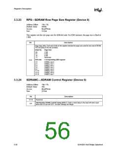
Register Description
Bit
Description
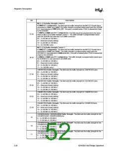
MECC [7:0] Buffer Strength Control 2.
4 DIMM FET Configuration: This field sets the buffer strength for the MECC[7:0] path that is
connected to DIMM2 and DIMM3 The buffer strength is programmable based upon the SDRAM
ECC load detected in DIMM slots 2&3. This path is enabled when FENA is deasserted (High)
by the 82443BX.
3 DIMM & 4 DIMM non-FET Configurations: This field should be programmed to the same
value as MECC[7:0] Buffer Strength Control 1. This buffer strength is programmable based
upon the SDRAM load detected in all DIMM connectors.
31:30
00 = 1x (66 MHz & 100 MHz)
01 = Reserved (Invalid setting)
10 = 2x (66 MHz & 100 MHz)
11 = 3x (100 MHz only)
MECC [7:0] Buffer Strength Control 1.
4 DIMM FET Configuration: This field sets the buffer strength for the MECC[7:0] path that is
connected to DIMM0 and DIMM1. The buffer strength is programmable based upon the
SDRAM ECC load detected in DIMM slots 0&1. This path is enabled when FENA is deasserted
(High) by the 82443BX.
3 DIMM & 4 DIMM non-FET Configuration: The buffer strength is programmable based upon
the SDRAM ECC load detected in all DIMM slots.
29:28
00 = 1x (66 MHz & 100 MHz)
01 = Reserved (Invalid setting)
10 = 2x (66 MHz & 100 MHz)
11 = 3x (100 MHz only)
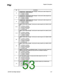
CSB7#/CKE5 Buffer Strength. This field sets the buffer strength for CSB7#/CKE5 pins.
00 = 1x (66 MHz & 100 MHz)
27:26
25:24
23:22
21:20
01 = Reserved (Invalid setting)
10 = 2x (66 MHz & 100 MHz)
11 = 3x (66 MHz & 100 MHz)
CSA7#/CKE3 Buffer Strength. This field sets the buffer strength for CSA7#/CKE3 pins.
00 = 1x (66 MHz & 100 MHz)
01 = Reserved (Invalid setting)
10 = 2x (66 MHz & 100 MHz)
11 = 3x (66 MHz & 100 MHz)
CSB6#/CKE4 Buffer Strength. This field sets the buffer strength for CSB6#/CKE4 pins.
00 = 1x (66 MHz & 100 MHz)
01 = Reserved (Invalid setting)
10 = 2x (66 MHz & 100 MHz)
11 = 3x (66 MHz & 100 MHz)
CSA6#/CKE2 Buffer Strength. This field sets the buffer strength for CSA6#/CKE2pins.
00 = 1x (66 MHz & 100 MHz)
01 = Reserved (Invalid setting)
10 = 2x (66 MHz & 100 MHz)
11 = 3x (66 MHz & 100 MHz)
CSA5#/RASA5#, CSB5#/RASB5# Buffer Strength. This field sets the buffer strength for the
CSA5#/RASA5#, CSB5#/RASB5# pins.
19
18
17
0 = 1x (66 MHz & 100 MHz)
1 = 2x (66 MHz & 100 MHz)
CSA4#/RASA4#, CSB4#/RASB4# Buffer Strength. This field sets the buffer strength for the
CSA4#/RASA4#, CSB4#/RASB4# pins.
0 = 1x (66 MHz & 100 MHz)
1 = 2x (66 MHz & 100 MHz)
CSA3#/RASA3#, CSB3#/RASB3# Buffer Strength. This field sets the buffer strength for the
CSA3#/RASA3#, CSB3#/RASB3# pins.
0 = 1x (66 MHz & 100 MHz)
1 = 2x (66 MHz & 100 MHz)
3-26
82443BX Host Bridge Datasheet

 ETC [ ETC ]