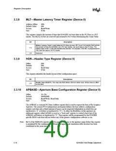
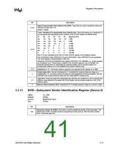
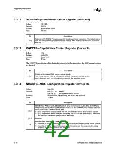
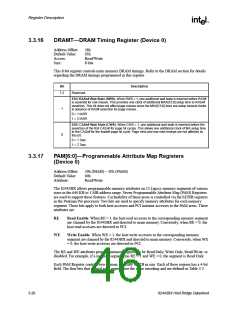
Register Description
Bit
Description
ECC - EDO static Drive mode.
0 = Normal mode of operation (default).
17
1 = ECC signals are always driven. This mode is used in a mobile system. EDO components are
used, but ECC components are not populated in any of the DRAM rows.
IDSEL_REDIRECT. This is a programmable option to make the 82443BX compatible with 430TX
base design. For CPU initiated configuration cycles to PCI, Device 1 which are targeted to the
82443BX’s host to AGP bridge:
0 = When set to ‘0’ (default), IDSEL1 (or AD12) is allocated to this bridge. The external AD12 is
never activated. CPU initiated configuration cycles to BUS0, DEVICE7 are targeted a PCI bus
device that its IDSEL input is connected to IDSEL7 (AD18).
16
1 = When set to ‘1’, IDSEL7 (or AD18) is allocated to this bridge. Since it is internal in the
82443BX, the external AD18 is never activated. CPU initiated configuration cycles to BUS0,
DEVICE7 are targeted a PCI bus device that its IDSEL input is connected to IDSEL1 (AD12).
In some 430TX based systems, this is connected to PIIX4E.
Note that CPU initiated configuration cycles to other PCI buses or other devices are normally
mapped and are not affected.
WSC# Handshake Disable. In the Uni-Processor mode, this bit should be set to ‘1’. In the Dual-
Processor mode where external IOAPIC is used, this bit should be set to ‘0’ (default). Setting this
bit to ‘0’, enables the WSC# handshake mechanism.
15
14
Intel Reserved.
Host/DRAM Frequency. These bits are used to determine the host and DRAM frequency. Bit 13
is set by an external strapping option at reset. These bits are also used to select the required
refresh rate. These bits apply to both SDRAM and EDO, with the exception that the setting ‘00’ for
100 MHz is illegal for an EDO system.
13:12
00 = 100 MHz
01 = Reserved
1 0 = 66 MHz
11 = Reserved
AGP to PCI Access Enable. When PHLDA# is active or there is an outstanding passive release
transaction pending: 1) this bit is set to 1 and the 82443BX allows AGP to PCI traffic, or 2) this bit
is set to 0 (default) and the 82443BX blocks AGP to PCI traffic. The AGP to PCI traffic must not
target the ISA bus.
11
10
1 = Enable
0 =Disable
PCI Agent to Aperture Access Disable. This bit is used to prevent access to the aperture from
the PCI side.
1 = Disable
0 = Enable (default). If this bit is “0” (default) and bit 9 = 1, accesses to the aperture are enabled
for the PCI side.
Note: This bit is don’t care if bit 9 of this register = 0.
Aperture Access Global Enable. This bit is used to prevent access to the aperture from any port
(CPU, PCI or AGP) before aperture range is established by the configuration software and
appropriate translation table in the main DRAM has been initialized. Default is “0”. It must be set
after system is fully configured for aperture accesses.
9
1 = Enable. Note that this bit globally controls accesses to the aperture. Once enabled, bit 10
provides the next level of control for accesses originated from the PCI side.
0 = Disable
DRAM Data Integrity Mode (DDIM) (R/W). These bits select one of 4 DRAM data integrity
modes.
00 = Non-ECC (Byte-Wise Writes supported) (Default)
01 = EC-only - Error Checking with No correction
10 = ECC Mode (Error Checking/Correction)
8:7
11 = ECC Mode with hardware scrubbing enabled
82443BX Host Bridge Datasheet
3-17

 ETC [ ETC ]