Register Description
3.3.12
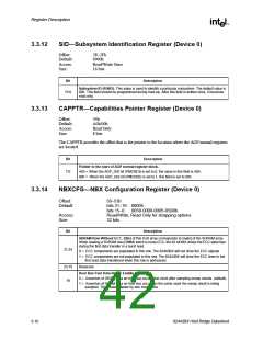
SID—Subsystem Identification Register (Device 0)
Offset:
Default:
Access:
Size:
2E–2Fh
0000h
Read/Write Once
16 bits
Bit
Description
Subsystem ID (R/WO). This value is used to identify a particular subsystem. The default value is
00h. This field should be programmed during boot-up. After this field is written once, it becomes
read only.
15:0
3.3.13
CAPPTR—Capabilities Pointer Register (Device 0)
Offset:
Default:
Access:
Size:
34h
A0h/00h
Read Only
8 bits
The CAPPTR provides the offset that is the pointer to the location where the AGP normal registers
are located.
Bit
Description
Pointer to the start of AGP normal register block.
7:0
A0h = When the AGP_DIS bit (PMCR[1]) is set to 0, the value in this field is A0h.
00h = When the AGP_DIS bit (PMCR[1]) is set to 1, this field is set to 00h.
3.3.14
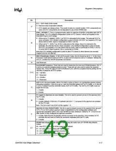
NBXCFG—NBX Configuration Register (Device 0)
Offset:
50–53h
Default:
bits 31–16: 0000h
bits 15–0: 00S0-0000-000S-0S00b
Read/Write, Read Only for strapping options
32 bits
Access:
Size:
Bit
Description
SDRAM Row Without ECC. Bit[n] of this 8 bit array corresponds to row[n] of the SDRAM array.
When reading a SDRAM row (DIMM) which is none-ECC, the 82 443BX drives the ECC data lines
during the first data transfer in a burst read.
31:24
0 = ECC components are populated in this row. The 82443BX will not drive the ECC signals.
1 = ECC components are not populated in this row. The 82443BX will drive the ECC lines in the
first read data transferred when this row is addressed.
23:19
18
Reserved.
Host Bus Fast Data Ready Enable (HBFDRE).
0 = Assertion of DRAM data on host bus occurs one clock after sampling snoop results. (default)
1 = Assertion of DRAM data on host bus occurs on the same clock the snoop result is being
sampled. This mode is faster by one clock cycle.
3-16
82443BX Host Bridge Datasheet

 ETC [ ETC ]