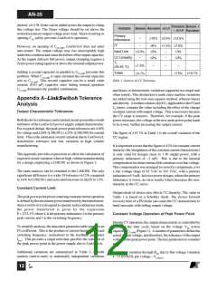
AN-35
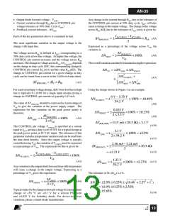
The overall tolerance is the sum of the deterministic variation
due to the change in line voltage and the change in the output
diode forward voltage with temperature, together with the root-
sum-square addition of the statistically independent circuit and
device variables.
Note that all of the above tolerances other than RFB and VC(IDCT)
arecompensatedoraccountedforinthepreviousanalysisofCC
tolerance. The contributions of RFB and VC(IDCT), since they are
unit-to-unit tolerances, have a very small influence (<0.1% on
the total sum of unit-to-unit tolerances).
In Equation A14 the ∆%LINE term ( 2.9%) is the expected
change in output voltage for a change of 90 VAC at 175 VAC,
the mid point of the specified input voltage range of 85 VAC to
265 VAC.
Constant Voltage Operation Below Peak Power Point
As the output load reduces from the peak power point, the
output voltage will tend to rise due to tracking errors compared
to the load terminals. Sources of these include the output cable
drop, output diode forward voltage and leakage inductance,
which is the dominant cause.
Equivalently, stating with the reference as 85 VAC, the output
voltage would increase +5.8% (twice 2.9%) when the input
increases to 265 VAC.
Astheloadreduces,theprimaryoperatingpeakcurrentreduces,
together with the leakage inductance energy, which reduces the
peak charging of CCLAMP. With a primary leakage inductance
figureof50µH, theoutputvoltagetypicallyrises40%fromfull
to no-load.
The analysis above is for a specific example, factors such as
diode choice, temperature range and output voltage can result
in a larger tolerance. However, for most cases the designer can
be confident the overall tolerance will be < 10%.
B
4/03
14

 ETC [ ETC ]