ZENTRUM MIKROELEKTRONIK DRESDEN AG
“ASI for you” IC
Datasheet
3
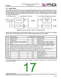
Detailed Functional Description
3.1 AS-i Receiver
The receiver detects (telegram) signals at the AS-i line, converts them to digital pulses and forwards them to the
UART for further processing. The receiver is internally connected between the ASIP and ASIN pins. It supports
floating (ground free) input signals within the voltage limits of ASIP and ASIN given in Table 2 at page 6.
Functional, the receiver removes the DC value of the input signal, band-pass filters the AC signal and extracts
the digital output signals from the sin2-shaped input pulses by a set of comparators. The amplitude of the first
pulse determines the threshold level for all following pulses. This amplitude is digitally filtered to guarantee sta-
ble conditions and to suppress burst spikes. This approach combines a fast adaptation to changing signal ampli-
tudes with a high detection safety. The comparators are reset after every detection of a telegram pause at the
AS-i line.
When the receiver is turned on, the transmitter is turned off to reduce the power consumption.
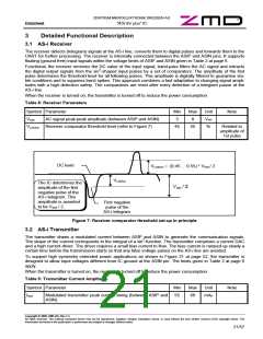
Table 8: Receiver Parameters
Symbol Parameter
Min
3
Max
8
Unit
VPP
%
Note
VSIG
AC signal peak-peak amplitude (between ASIP and ASIN)
VLSIGon Receiver comparator threshold level (refer to Figure 7)
45
55
Related to
amplitude of
1st pulse
DC level
VLSIGon = (0.45 ... 0.55) * VSIG / 2
VLSIGon
The IC determines the
VSIG / 2
amplitude of the first
negative pulse of the
AS-i telegram. This
amplitude is asserted
to be VSIG / 2.
First negative
pulse of the
AS-i telegram
Figure 7: Receiver comparator threshold set-up in principle
3.2 AS-i Transmitter
The transmitter draws a modulated current between ASIP and ASIN to generate the communication signals.
The shape of the current corresponds to the integral of a sin2-function. The transmitter comprises a current DAC
and a high current driver. The driver requires a small bias current to flow. The bias current is ramped up slowly a
certain time before the transmission starts so that any false voltage pulses on the AS-i line are avoided.
To support high symmetry extended power applications as shown in Figure 21 at page 52, the transmitter is
designed to allow input voltages different from IC ground at the ASIN pin. The limits given in Table 2 at page 6
apply.
When the transmitter is turned on, the receiver is turned off to reduce the power consumption.
Table 9: Transmitter Current Amplitude
Symbol Parameter
ISIG Modulated transmitter peak current swing (between ASIP and
Min
55
Max
68
Unit
mAP
Note
ASIN)
Copyright © 2006, ZMD AG, Rev.1.4
All rights reserved. The material contained herein may not be reproduced, adapted, merged, translated, stored, or used without the prior written consent of the copyright owner. The
Information furnished in this publication is preliminary and subject to changes without notice.
21/57

 ZMD [ Zentrum Mikroelektronik Dresden AG ]