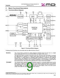
ZENTRUM MIKROELEKTRONIK DRESDEN AG
“ASI for you” IC
Datasheet
The data port is accompanied by the data strobe signal DSR. There is a defined phase relation between a data
output event, the input data sampling and the activation of the DSR signal. Thus, it can be used to trigger exter-
nal logic or a micro controller to process the received data or to provide new input data for the AS-i slave re-
sponse. See chapter 3.7 Data Port and DSR on page 29 for further details.
2.3.5 Data Input Inversion
By default the logic signal (HIGH / LOW) that is present at the data input pins during the input sampling phase is
transferred without modification to the send register, which is interfaced by the UART. By that, the signal be-
comes directly part of the slave response.
Some applications work with inverted logic levels. To avoid additional external inverters, the input signal can be
inverted by the ASI4U before transferring it to the send register. The inversion of the input signals can either be
done bit selective or jointly for all data input pins. See chapter 3.7.2 Input Data Pre-Processing on page 30.
2.3.6 Data Input Filtering
To prevent input signal bouncing from being transferred to the AS-i Master, the data input signals can be digi-
tally filtered. Filter times can be configured in 7 steps from 128µs up to 8.192ms. Additionally there is a so called
AS-i Cycle Mode available. If activated, the filter time is determined by the actual AS-i cycle time. For more de-
tailed information refer to chapter 3.7.2 Input Data Pre-Processing on page 30.
The filter function can be enabled bit selective. Activation of the filters is done jointly either by E²PROM configu-
ration or by the logic state of parameter port pin P2. See chapter 3.7.2 Input Data Pre-Processing on page 30.
2.3.7 Fixed Data Output Driving
The fixed data output driving feature is thought to ease board level design for similar products that do not re-
quire the full data output port width. The user can select one or more bits from the data output port to be driven
by a distinct logic level instead by the data that was sent by the master. The distinct output data is stored in the
E²PROM and can be set during final module configuration. Thus it is possible to signal the actual IC profile to
some external circuitry and to allow reuse of certain board designs for different product applications.
See chapter 3.7.3 Fixed Output Data Driving on page 32 for further details.
2.3.8 Synchronous Data I/O Mode
AS-i Complete Specification V3.0 newly defines a synchronous data I/O feature, that allows a number of slaves
in the network to switch their outputs at the same time and to have their inputs sampled jointly. This feature is
especially useful if more than 4-bit wide data is to be provided synchronously to an application.
The synchronization point was defined to the data exchange event of the slave with the lowest address in the
network. This definition relies on the cyclical slave polling with increasing slave addresses per cycle that is one
of the basic communication principles of AS-i. The IC always monitors the data communication and detects the
change from a higher to a lower slave address. If such a change was recognized, the IC assumes that the slave
with the lower address has the lowest address in the network.
There are some special procedures that become active during the start of synchronous I/O mode operation and
if more than three consecutive telegrams were sent to the same slave address. This is described in more detail
in chapter 3.7.4 Synchronous Data I/O Mode on page 32.
2.3.9 4 Input / 4 Output processing in Extended Address Mode
A new feature of AS-i Complete Specification v3.0 is also support of 4-bit wide output data in Extended Address
Mode. In Extended Address Mode it was, up to Complete Specification v2.11, only possible to send three data
output bits from the master to the slave because telegram bit I3 is used to select between A- and B- slave type
for extended slave addressing (up to 62 slaves per network). In normal address mode I3 carries output data for
pin D3.
The new definition introduces a multiplexed data transfer, so that all 4-bits of the data output port can be used
again. A first AS-i cycle transfers the data for a 2-bit output nibble only, while the second AS-i cycle transfers the
data for the contrary 2-bit nibble. Nibble selection is done by the remaining third bit. To ensure continuous alter-
nation of bit information I2 and thus continued data transfer to both nibbles, a special watchdog was imple-
mented that observes the state of I2 bit. The watchdog can be activated or deactivated by E²RPOM setting. It
provides a watchdog filter time of about 327ms.
Copyright © 2006, ZMD AG, Rev.1.4
All rights reserved. The material contained herein may not be reproduced, adapted, merged, translated, stored, or used without the prior written consent of the copyright owner. The
Information furnished in this publication is preliminary and subject to changes without notice.
13/57

 ZMD [ Zentrum Mikroelektronik Dresden AG ]