<ꢀ5ꢁꢀꢂꢃ<ꢀ.ꢁꢀꢂ
'PJCPEGFꢄ<ꢁꢀꢂꢄ/KETQRTQEGUUQT
ZiLOG
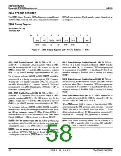
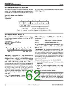
+06'44726ꢄ8'%614ꢄ.19ꢄ4')+56'4
Bits ꢊ ꢏ of the Interrupt Vector Low Register (+ ) are used
as bits ꢊ ꢏ of the synthesized interrupt vector during inter-
rupts for the +06ꢄ and +06ꢂ pins and for the DMAs, ASCIs,
PRTs, and CSI/O. These three bits are cleared toꢅ0during
4'5'6 (Figure 74).
+PVGTTWRVꢄ8GEVQTꢄ.QYꢄ4GIKUVGT
/PGOQPKEꢅꢄ+.
#FFTGUUꢄꢋꢋ*
ꢎ
ꢄ
ꢊ
ꢁ
ꢂ
ꢀ
ꢏ
ꢍ
$KV
+.ꢅꢁ
+.ꢅꢊ
4ꢌ9
+.ꢅꢏ
4ꢌ9
4ꢌ9
2TQITCOOCDNG
+PVGTTWRVꢅ5QWTEGꢅ&GRGPFGPVꢅ%QFG
(KIWTG ꢐꢉꢆ +PVGTTWRVꢄ8GEVQTꢄ.QYꢄ4GIKUVGTꢄꢌ+.ꢅꢄ+ꢃ1ꢄ#FFTGUUꢄꢒꢄꢋꢋ*ꢍ
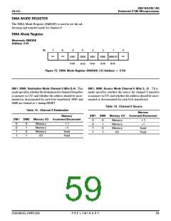
+06ꢃ64#2ꢄ%10641.ꢄ4')+56'4
This register is used in handling 64#2 interrupts and to en-
able or disable Maskable Interrupt Levelꢅꢀꢅand the +06ꢄ
and +06ꢂ pins.
+06ꢂ and +06ꢄ, respectively. +6'ꢀ enables and disables in-
terrupts from:
'5%%
%6%U
• Bidirectional Centronics controller
+06ꢃ64#2ꢄ%QPVTQNꢄ4GIKUVGT
/PGOQPKEUꢄ+6%
#FFTGUUꢄꢋꢉ*
• External interrupt input +06ꢀ
A 1 in a bit enables the corresponding interrupt level while
aꢅ0disables it. A 4'5'6 sets +6'ꢀ to 1 and clears +6'ꢄ
and +6'ꢂ to 0.
ꢎ
ꢊ
ꢁ
ꢂ
ꢄ
ꢀ
ꢏ
ꢍ
$KV
64#2
7(1
+6'ꢂ +6'ꢄ
+6'ꢀ
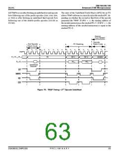
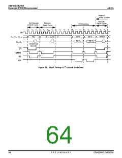
64#2ꢄ+PVGTTWRVꢆꢄThe Z8S180/Z8L180 generates a 64#2
sequence when an undefined opcode fetch occurs. This fea-
ture can be used to increase software reliability, implement
an extended instruction set, or both. 64#2 may occur during
opcode fetch cycles and also if an undefined opcode is
fetched during the interrupt acknowledge cycle for +06ꢀ
when Modeꢅꢀꢅis used.
4ꢌ9
4
4ꢌ9 4ꢌ9 4ꢌ9
64#2ꢄꢌ$KVꢄꢐꢍꢆꢄThis bit is set to 1 when an undefined op-
code is fetched. 64#2 can be reset under program control
bywritingitwithaꢀ;however,64#2cannotbewrittenwith
1 under program control. 64#2 is reset toꢅ0during 4'5'6.
When a 64#2 sequence occurs, the Z8S180/Z8L180:
7(1ꢅꢄ7PFGHKPGFꢄ(GVEJꢄ1DLGEVꢄꢌ$KVꢄꢈꢍꢆꢄWhen a 64#2 in-
terrupt occurs, the contents of 7(1 allow the starting ad-
dress of the undefined instruction to be determined. This in-
terrupt is necessary because the 64#2 may occur on either
the second or third byte of the opcode. 7(1 allows the
stacked PC value to be correctly adjusted. If 7(1ꢅꢐꢅ0, the
first opcode should be interpreted as the stacked 2%ꢃꢄ. If
7(1ꢅꢐ 1, the first opcode address is stacked 2%ꢃꢂ. 7(1 is
Read-Only.
1. Sets the 64#2 bit in the Interrupt 64#2/Control (+6%)
register to 1.
2. Saves the current Program Counter (PC) value,
reflecting the location of the undefined opcode, on the
stack.
3. Resumes execution at logical address 0.
0QVGꢅ If logical address 0000His mapped to physical address
00000H, the vector is the same as for 4'5'6. In this
case, testing the 64#2 bit in +6% reveals whether the re-
start at physical address 00000Hwas caused by 4'5'6
or 64#2.
+6'ꢇꢎꢄꢁꢎꢄꢂꢅꢄ+PVGTTWRVꢄ'PCDNGꢄꢇꢎꢄꢁꢎꢄꢂꢄꢌ$KVUꢄꢇ ꢂꢍꢆꢄ+6'ꢂ
and +6'ꢄ enable and disable the external interrupt inputs
ꢁꢂ
2ꢅ4ꢅ'ꢅ.ꢅ+ꢅ/ꢅ+ꢅ0ꢅ#ꢅ4ꢅ;
&5ꢀꢀꢁꢀꢀꢂꢃ</2ꢀꢂꢀꢀ

 ZILOG [ ZILOG, INC. ]