<ꢀ5ꢁꢀꢂꢃ<ꢀ.ꢁꢀꢂ
'PJCPEGFꢄ<ꢁꢀꢂꢄ/KETQRTQEGUUQT
ZiLOG
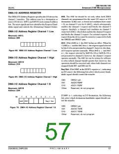
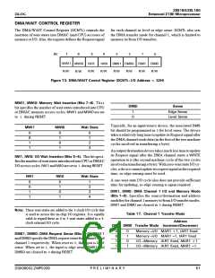
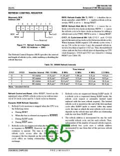
&/#ꢃ9#+6ꢄ%10641.ꢄ4')+56'4
The DMA/WAIT Control Register (&%06.) controls the
insertion of wait states into DMAC (and CPU) accesses of
memory or I/O. Also, the register defines the Request signal
for each channel as level or edge sense. &%06. also sets
the DMA transfer mode for channel 1, which is limited to
memory to/from I/O transfers.
ꢏ
ꢎ
ꢍ
ꢄ
$KV
ꢊ
ꢁ
ꢂ
ꢀ
/9+ꢄ
4ꢌ9
/9+ꢀ
4ꢌ9
+9+ꢀ
4ꢌ9
&/5ꢀ
4ꢌ9
&+/ꢀ
4ꢌ9
+9+ꢄ
4ꢌ9
&/5ꢄ
4ꢌ9
&+/ꢄ
4ꢌ9
(KIWTG ꢐꢋꢆ &/#ꢃ9#+6ꢄ%QPVTQNꢄ4GIKUVGTꢄꢌ&%06.ꢅꢄ+ꢃ1ꢄ#FFTGUUꢄꢒꢄꢋꢇ*ꢍ
/9+ꢁꢎꢄ/9+ꢂꢅꢄ/GOQT[ꢄ9CKVꢄ+PUGTVKQPꢄꢌ$KVUꢄꢐ ꢈꢍꢆꢄThis
&/5K
5GPUG
bit specifies the number of wait states introduced into CPU
or DMAC memory access cycles. /9+ꢄ and /9+ꢀ are set
to 1 during 4'5'6.
ꢄ
ꢀ
'FIGꢅ5GPUG
.GXGNꢅ5GPUG
Typically, for an input/source device, the associated &/5
bit should be programmed asꢅ0for level sense. The device
takes a relatively long time to update its Request signal after
the DMA channel reads data (in the first of the two machine
cycles involved in transferring a byte).
/9+ꢁ
/9+ꢂ
9CKVꢄ5VCVG
ꢀ
ꢀ
ꢄ
ꢄ
ꢀ
ꢄ
ꢀ
ꢄ
ꢀ
ꢄ
ꢂ
ꢍ
Anoutput/destinationdevice takesmuchlesstimetoupdate
its Request signal after the DMA channel starts a 94+6'
operation to it (the second machine cycle of the two cycles
involvedintransferringabyte). Withzero-wait stateI/Ocy-
cles, a devicecannotupdateitsrequest signalin the required
time, so edge sensing must be used.
+9+ꢁꢎꢄ+9+ꢂꢅꢄ+ꢃ1ꢄ9CKVꢄ+PUGTVKQPꢄꢌ$KVUꢄꢑ ꢉꢍꢆꢄThis bit speci-
fies the number of wait states introduced into CPU or DMAC
I/Oaccess cycles. +9+ꢄ and +9+ꢀ are set to
1
during 4'5'6.
+9+ꢁ
+9+ꢂ
9CKVꢄ5VCVG
A one-wait-state I/O cycle also does not provide sufficient
time for updating, so edge sensing is again required.
ꢀ
ꢀ
ꢄ
ꢄ
ꢀ
ꢄ
ꢀ
ꢄ
ꢄ
ꢂ
ꢍ
ꢎ
&+/ꢁꢎꢄ&+/ꢂꢅꢄ&/#ꢄ%JCPPGNꢄꢁꢄ+ꢃ1ꢄCPFꢄ/GOQT[ꢄ/QFG
ꢌ$KVUꢄꢁ ꢂꢍꢆꢄSpecifies the source/destination and address
modifier for channel 1 memory to/from I/O transfer modes.
&+/ꢄ and &+/ꢀ are cleared toꢅ0during 4'5'6.
0QVGꢅ These wait states are added to the 3-clock I/O cycle that
is used to access the on-chip I/O registers. It is equally
valid to regard these as 0 to 3 wait states added to a 4-
clock external I/O cycle.
6CDNG ꢁꢐꢆ %JCPPGNꢄꢁꢄ6TCPUHGTꢄ/QFG
#FFTGUUꢄ
&+/ꢁ &/+ꢂ 6TCPUHGTꢄ/QFG +PETGOGPVꢃ&GETGOGPV
ꢀ
ꢀ
ꢄ
ꢄ
ꢀ
ꢄ
ꢀ
ꢄ
/GOQT[→+ꢌ1 /#4ꢄꢅꢔꢄꢇꢅ+#4ꢄꢅHKZGF
/GOQT[→+ꢌ1 /#4ꢄꢅ ꢄꢇꢅ+#4ꢄꢅHKZGF
+ꢌ1→/GOQT[ +#4ꢄꢅHKZGFꢇꢅ/#4ꢄꢅꢔꢄ
+ꢌ1→/GOQT[ +#4ꢄꢅHKZGFꢇꢅ/#4ꢄꢅ ꢄ
&/5ꢁꢎꢄ&/5ꢂꢅꢄ&/#ꢄ4GSWGUVꢄ5GPUGꢄꢌ$KVUꢄꢋ ꢇꢍꢆꢄ&/5ꢄ
and&/5ꢀ specifytheDMArequestsenseforchannel 0and
channel 1 respectively. When reset toꢅ0, the input is level
sense. When set to 1, the input is edge sense. &/5ꢄ and
&/5ꢀ are cleared toꢅ0during 4'5'6.
&5ꢀꢀꢁꢀꢀꢂꢃ</2ꢀꢂꢀꢀ
2ꢅ4ꢅ'ꢅ.ꢅ+ꢅ/ꢅ+ꢅ0ꢅ#ꢅ4ꢅ;
ꢁꢄ

 ZILOG [ ZILOG, INC. ]