<ꢀ5ꢁꢀꢂꢃ<ꢀ.ꢁꢀꢂ
'PJCPEGFꢄ<ꢁꢀꢂꢄ/KETQRTQEGUUQT
ZiLOG
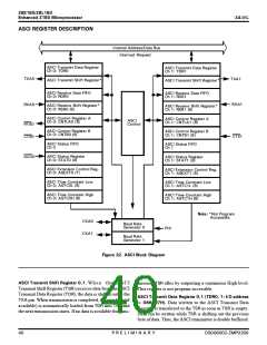
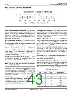
#5%+ꢄ%*#00'.ꢄ%10641.ꢄ4')+56'4ꢄ$
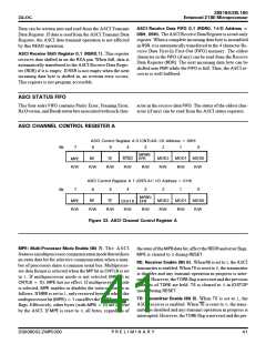
#5%+ꢅ%QPVTQNꢅ4GIKUVGTꢅ$ꢅꢀꢅꢈ%06.$ꢀꢓꢅ+ꢌ1ꢅ#FFTGUUꢅꢐꢅꢀꢂ*ꢉ
#5%+ꢅ%QPVTQNꢅ4GIKUVGTꢅ$ꢅꢄꢅꢈ%06.$ꢄꢓꢅ+ꢌ1ꢅ#FFTGUUꢅꢐꢅꢀꢍ*ꢉ
ꢂ
ꢄ
$KV
ꢏ
ꢍ
ꢊ
ꢁ
ꢎ
ꢀ
%65ꢌ
25
/2
ꢅ/2$6
4ꢌ9
2'1
4ꢌ9
&4
55ꢂ
4ꢌ9
55ꢄ
4ꢌ9
55ꢀ
4ꢌ9
4ꢌ9
4ꢌ9
4ꢌ9
(KIWTG ꢋꢉꢆ #5%+ꢄ%JCPPGNꢄ%QPVTQNꢄ4GIKUVGTꢄ$
/2$6ꢅꢄ/WNVKRTQEGUUQTꢄ$KVꢄ6TCPUOKVꢄꢌ$KVꢄꢐꢍꢆꢄWhen multi-
processor communication format is selected (/2 bit = ꢄ),
/2$6 is used to specify the /2$ data bit for transmission.
If /2$6ꢅꢐ 1, then /2$ꢅꢐꢅꢄ is transmitted. If /2$6ꢅꢐ
0, then /2$ꢅꢐꢅ0is transmitted. The /2$6 state is unde-
fined during and after 4'5'6.
2'1ꢅꢄ2CTKV[ꢄ'XGPꢄ1FFꢄꢌ$KVꢄꢉꢍꢄꢆꢄ2'1 selects oven or odd
parity. 2'1 does not affect the enabling/disabling of parity
(/1&ꢄ bit of %06.#). If 2'1 is cleared toꢅ0, even parity
is selected. If 2'1 is set to 1, odd parity is selected. 2'1 is
cleared toꢅ0during 4'5'6.
&4ꢅꢄ&KXKFGꢄ4CVKQꢄꢌ$KVꢄꢋꢍꢆꢄIf the :ꢄ bit in the #5':6 reg-
ister isꢅ0, this bit specifies the divider used to obtain baud
rate from the data sampling clock. If &4 is reset toꢅ0, divide-
by-16 is used, while if &4 is set to 1, divide-by-64 is used.
&4 is cleared toꢅ0during 4'5'6.
/2ꢅꢄ/WNVKRTQEGUUQTꢄ/QFGꢄꢌ$KVꢄꢈꢍꢆꢄWhen /2 is set to 1,
thedataformatisconfiguredformultiprocessormodebased
on /1&ꢂ (number of data bits) and /1&ꢀ (number of stop
bits) in %06.#. The format is as follows:
5VCTVꢅDKVꢅꢔꢅꢊꢅQTꢅꢆꢅFCVCꢅDKVUꢅꢔꢅ/2$ꢅDKVꢅꢔꢅꢄꢅQTꢅꢂꢅUVQRꢅDKVU
55ꢇꢎꢁꢎꢂꢅꢄ5QWTEGꢃ5RGGFꢄ5GNGEVꢄꢇꢎꢁꢎꢂꢄꢌ$KVUꢄꢇ ꢂꢍꢆꢄFirst,
if these bits are ꢄꢄꢄ, as they are after a 4'5'6, the %-#
pin is used as a clock input, and is divided by 1, 16, or 64
depending on the &4 bit and the :ꢄ bit in the #5':6 reg-
ister.
Multiprocessor (/2ꢅꢐꢅꢄ) format offers no provision for
parity. If /2ꢅꢐꢅ0, the data format is based on /1&ꢀ,
/1&ꢄ, /1&ꢂ, and may include parity. The /2 bit is
cleared toꢅ0during 4'5'6.
If these bits are not ꢄꢄꢄ and the $4) mode bit is #5':6
isꢅ0, then these bits specify a power-of-two divider for the
2*+ clock as indicated in Table 10.
%65ꢃ25ꢅꢄ%NGCTꢄVQꢄ5GPFꢃ2TGUECNGꢄꢌ$KVꢄꢑꢍꢆꢄWhen read,
%65ꢌ25 reflects the state of the external %65 input. If the
%65 input pin is High, %65ꢌ25 is read as 1.
Setting or leaving these bits as ꢄꢄꢄ makes sense for a chan-
nel only when its %-# pin is selected for the %-# function.
%-#1ꢌ%-5 offers the%-#1 functionwhenbit4oftheSys-
tem Configuration Register is 0. &%&ꢀ/%-#ꢄ offers the
%-#ꢄ functionwhenbitꢅ0of theInterruptEdgeregisteris1.
0QVGꢅ When the %65 input pin is High, the 6&4' bit is inhib-
ited (that is, held at ꢀ).
For channel 1, the %65 input is multiplexed with 4:5 pin
(Clocked Serial Receive Data). Thus, %65ꢌ25 is only valid
when read if the channel 1 %65ꢄ' bit = 1 and the %65
input pin function is selected. The 4'#& data of %65ꢌ25
is not affected by 4'5'6.
6CDNG ꢁꢂꢆ &KXKFGꢄ4CVKQ
55ꢇ
55ꢁ
55ꢂ
&KXKFGꢄ4CVKQ
ꢀ
ꢀ
ꢀ
ꢀ
ꢄ
ꢄ
ꢄ
ꢄ
ꢀ
ꢀ
ꢄ
ꢄ
ꢀ
ꢀ
ꢄ
ꢄ
ꢀ
ꢄ
ꢀ
ꢄ
ꢀ
ꢄ
ꢀ
ꢄ
÷ꢄ
÷ꢂ
÷ꢎ
÷ꢆ
÷ꢄꢁ
If the 55ꢂ ꢀ bits in this register are not ꢄꢄꢄ, and the $4)
mode bit in the #5':6 register isꢅ0, then writing to this bit
sets the prescale (PS) control. Under those circumstances,
aꢅ0indicates a divide-by-10 prescale function while a 1
indicates divide-by-30. The bit resets to 0.
÷ꢍꢂ
÷ꢁꢎ
'ZVGTPCNꢅ%NQEM
&5ꢀꢀꢁꢀꢀꢂꢃ</2ꢀꢂꢀꢀ
2ꢅ4ꢅ'ꢅ.ꢅ+ꢅ/ꢅ+ꢅ0ꢅ#ꢅ4ꢅ;
ꢎꢍ

 ZILOG [ ZILOG, INC. ]