<ꢀ5ꢁꢀꢂꢃ<ꢀ.ꢁꢀꢂ
'PJCPEGFꢄ<ꢁꢀꢂꢄ/KETQRTQEGUUQT
ZiLOG
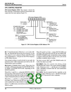
$KVꢄꢇꢄ.0+1ꢆꢄThis bit controls the drive capability of certain
external I/O pins of the Z8S180/Z8L180. When this bit is
set to 1, the output drive capability of the following pins is
reduced to 33 percent of the original drive capability:
$KVꢄꢁꢄ.0%27%6.ꢆꢄThis bit controls the drive capability of
the CPU Control pins. When this bit is set to 1, the output
drive capability of the following pins is reduced to 33 per-
cent of the original drive capability:
465ꢀ
6Z5
$75#%-
94
4&
%-#ꢄꢌ6'0&ꢀ
6:#ꢀ
%-#ꢀꢌ&4'3ꢀ
6:#ꢄ
/ꢄ
/4'3
4(5*
'
+143
*#.6
6'56
6'0&K
%-5
56
$KVꢄꢂꢄ.0#&ꢃ#ꢆꢄThis bit controls the drivecapability of
the Address/Data bus output drivers. If this bit is set to 1,
the output drive capability of the Address and Data bus out-
puts is reduced to 33 percent of its original drive capability.
&5ꢀꢀꢁꢀꢀꢂꢃ</2ꢀꢂꢀꢀ
2ꢅ4ꢅ'ꢅ.ꢅ+ꢅ/ꢅ+ꢅ0ꢅ#ꢅ4ꢅ;
ꢍꢋ

 ZILOG [ ZILOG, INC. ]