<ꢀ5ꢁꢀꢂꢃ<ꢀ.ꢁꢀꢂ
'PJCPEGFꢄ<ꢁꢀꢂꢄ/KETQRTQEGUUQT
ZiLOG
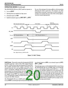
+&.'ꢅ/QFG
$WUꢅ4GNGCUGꢅ/QFG
+&.'ꢅ/QFG
6:
6:
2*+
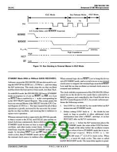
ꢋꢑꢏꢅ%[ENGꢅ&GNC[ꢅWPVKNꢅ$75#%-ꢅ#UUGTVGF
$754'3
$75#%-
#
#
(((((*
(((((*
*KIJꢅ+ORGFCPEG
*KIJ
*#.6
/ꢄ
.QY
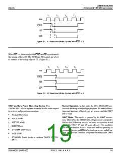
(KIWTG ꢁꢈꢆ $WUꢄ)TCPVKPIꢄVQꢄ'ZVGTPCNꢄ/CUVGTꢄKPꢄ+&.'ꢄ/QFG
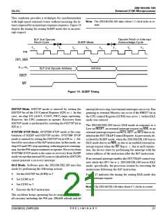
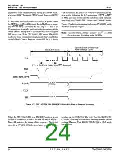
56#0&$;ꢄ/QFGꢄꢌ9KVJꢄQTꢄ9KVJQWVꢄ37+%-ꢄ4'%18'4;ꢍꢆ
When external logic drives 4'5'6 Low to bring the device
out of 56#0&$; mode, and a crystal is in use or an external
clock source is stopped, the external logic must hold4'5'6
Low until the on-chip oscillator or external clock source is
restarted and stabilized.
Software canput the Z8S180/Z8L180 into this mode by set-
ting the +15612 bit (ICR5) toꢅ1, CCR6 toꢅ1, and executing
the 5.2 instruction. This mode stops the on-chip oscillator
and thus draws the least power of any mode, less than 10µA.
Theclock-stabilityrequirementsoftheZ8S180/Z8L180are
much less in the divide-by-two mode that is selected by a
4'5'6 sequence and controlled by the Clock Divide bit in
theCPUControlRegister(CCR7). Asaresult, softwareper-
forms the following actions:
As with +&.' mode, the Z8S180/Z8L180 leaves 56#0&$;
mode in response to a Low on 4'5'6, on 0/+, or a Low
on +06ꢀ–2 that is enabled by a 1 in the corresponding bit
in the INT/TRAP Control Register. This action grants the
bus to an external Master if the BREXT bit in the CPU Con-
trol Register (CCR5) is 1. The time required for all of these
operations is greatly increased by the necessity for restart-
ing the on-chip oscillator, and ensuring that it stabilizes to
square-wave operation.
1. Sets CCR7 toꢅ0for divide-by-two mode before an 5.2
instruction and 56#0&$; mode.
2. Delays setting CCR7 back to 1 for divide-by-one
mode as long as possible to allow additional clock
stabilization time after a 4'5'6, interrupt, or in-line
RESTART after an 5.2 01 instruction.
WhenanexternalclockisconnectedtotheEXTALpinrath-
er than a crystal to the XTAL and EXTAL pins and the ex-
ternal clockrunscontinuously, there is little necessity to use
56#0&$; mode because no time is required to restart the
oscillator, and other modes restart faster. However, if ex-
ternal logic stops the clock during 56#0&$; mode (for ex-
ample, by decoding *#.6 Low and /ꢄ High for several
clock cycles), then 56#0&$; mode can be useful to allow
the external clock source to stabilize after it is re-enabled.
If CCR6 is set to 1 before the 5.2 instruction places the
MPU in 56#0&$; mode, the value of the CCR3 bit deter-
mines the length of the delay before the oscillator restarts
and stabilizes when it leaves 56#0&$; mode due to an ex-
ternal interrupt request. When CCR3 isꢅ 0, the
17
Z8S180/Z8L180 waits 2 (131,072) clock cycles. When
CCR3 isꢅ1, it waits 64 clock cycles. This state is called
37+%-ꢅ4'%18'4; mode. The same delay applies to grant-
&5ꢀꢀꢁꢀꢀꢂꢃ</2ꢀꢂꢀꢀ
2ꢅ4ꢅ'ꢅ.ꢅ+ꢅ/ꢅ+ꢅ0ꢅ#ꢅ4ꢅ;
ꢂꢍ

 ZILOG [ ZILOG, INC. ]