<ꢀ5ꢁꢀꢂꢃ<ꢀ.ꢁꢀꢂ
'PJCPEGFꢄ<ꢁꢀꢂꢄ/KETQRTQEGUUQT
ZiLOG
6
6
6
6
2*+
+143
4&
94
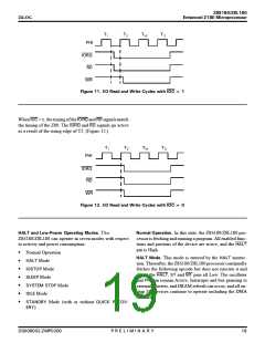
(KIWTG ꢁꢁꢆ +ꢃ1ꢄ4GCFꢄCPFꢄ9TKVGꢄ%[ENGUꢄYKVJꢄ+1%ꢄꢒꢄꢁ
When+1% =ꢅ0, the timing of the +143 and 4& signals match
the timing of the Z80. The +143 and 4& signals go active
as a result of the rising edge of T2. (Figure 12.)
6
6
6
6
2*+
+143
4&
94
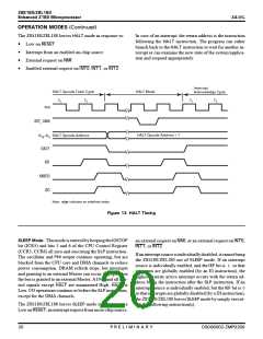
(KIWTG ꢁꢇꢆ +ꢃ1ꢄ4GCFꢄCPFꢄ9TKVGꢄ%[ENGUꢄYKVJꢄ+1%ꢄꢒꢄꢂ
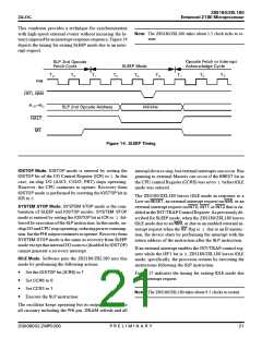
*#.6ꢄCPFꢄ.QYꢊ2QYGTꢄ1RGTCVKPIꢄ/QFGUꢆꢄThe
Z8S180/Z8L180 can operate in seven modes with respect
to activity and power consumption:
0QTOCNꢄ1RGTCVKQPꢆꢄIn this state, the Z8S180/Z8L180 pro-
cessor is fetching and running a program. All enabled func-
tions and portions of the device are active, and the *#.6
pin is High.
Normal Operation
*#.6ꢄ/QFGꢆꢄThis mode is entered by the *#.6 instruc-
tion. Thereafter, the Z8S180/Z8L180 processor continually
fetches the following opcode but does not execute it and
drives the *#.6, 56 and /ꢄ pins all Low. The oscillator
and 2*+ pin remain Active. Interrupts and bus granting to
external Masters, and DRAM refresh can occur, and all on-
chip I/O devices continue to operate including the DMA
channels.
*#.6 Mode
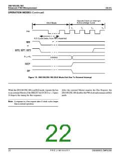
+15612 Mode
5.''2 Mode
5;56'/ꢅ5612 Mode
+&.' Mode
56#0&$; Mode (with or without 37+%-ꢅ 4'%18ꢃ
'4;
)
&5ꢀꢀꢁꢀꢀꢂꢃ</2ꢀꢂꢀꢀ
2ꢅ4ꢅ'ꢅ.ꢅ+ꢅ/ꢅ+ꢅ0ꢅ#ꢅ4ꢅ;
ꢄꢋ

 ZILOG [ ZILOG, INC. ]