<ꢀ5ꢁꢀꢂꢃ<ꢀ.ꢁꢀꢂ
'PJCPEGFꢄ<ꢁꢀꢂꢄ/KETQRTQEGUUQT
ZiLOG
56#0&ꢄ6'56ꢄ%10&+6+105
The following standard test conditions apply to DC Char-
acteristics, unless otherwise noted. All voltages are refer-
enced to V (0V). Positive current flows into the refer-
SS
enced pin.
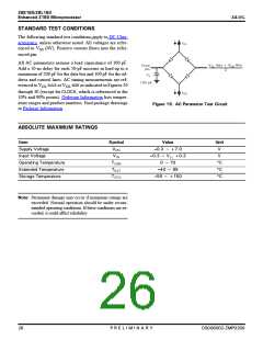
All AC parameters assume a load capacitance of 100 pF.
Add a 10-ns delay for each 50-pF increase in load up to a
maximum of 200 pF for the data bus and 100 pF for the ad-
dress and control lines. AC timing measurements are ref-
erenced to V MAX or V MIN as indicated in Figures 20
OL
OL
through 30 (except for %.1%-, which is referenced to the
10% and 90% points). Ordering Information lists temper-
ature ranges and product numbers. Find package drawings
in Package Information.
(KIWTG ꢁꢏꢆ #%ꢄ2CTCOGVGTꢄ6GUVꢄ%KTEWKV
#$51.76'ꢄ/#:+/7/ꢄ4#6+0)5
+VGO
5[ODQN
8CNWG
ꢀꢑꢍꢅ`ꢅꢔꢊꢑꢀ
ꢀꢑꢍꢅ`ꢅ8 ꢅꢔꢀꢑꢍ
ꢀꢅ`ꢅꢊꢀ
7PKV
8
5WRRN[ꢅ8QNVCIG
+PRWVꢅ8QNVCIG
8
8
6
8
1RGTCVKPIꢅ6GORGTCVWTG
'ZVGPFGFꢅ6GORGTCVWTG
5VQTCIGꢅ6GORGTCVWTG
u%
u%
u%
6
ꢎꢀꢅ`ꢅꢆꢏ
6
ꢏꢏꢅ`ꢅꢔꢄꢏꢀ
0QVGꢅ Permanent damage may occur if maximum ratings are
exceeded. Normal operation should be under recom-
mended operating conditions. If these conditions are ex-
ceeded, it could affect reliability.
ꢂꢁ
2ꢅ4ꢅ'ꢅ.ꢅ+ꢅ/ꢅ+ꢅ0ꢅ#ꢅ4ꢅ;
&5ꢀꢀꢁꢀꢀꢂꢃ</2ꢀꢂꢀꢀ

 ZILOG [ ZILOG, INC. ]