eZ80L92 MCU
Product Specification
177
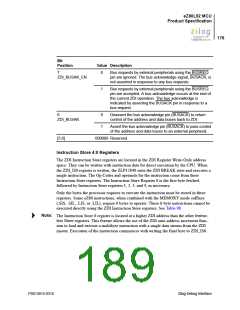
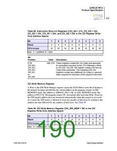
Table 98. Instruction Store 4:0 Registers (ZDI_IS4 = 21h, ZDI_IS3 = 22h,
ZDI_IS2 = 23h, ZDI_IS1 = 24h, and ZDI_IS0 = 25h in the ZDI Register Write-
Only Address Space)
Bit
7
X
6
X
5
X
4
X
3
X
2
X
1
X
0
X
Reset
CPU Access
W
W
W
W
W
W
W
W
Note: X = Undefined; W = Write.
Bit
Position
Value Description
[7:0]
00h–FFh These registers contain the Op Codes and operands
for immediate execution by the CPU following a Write
to ZDI_IS0. The ZDI_IS0 register contains the first Op
Code of the instruction. The remaining ZDI_ISx
ZDI_IS4,
ZDI_IS3,
ZDI_IS2,
ZDI_IS1,
or
registers contain any additional Op Codes or operand
dates required for execution of the required instruction.
ZDI_IS0
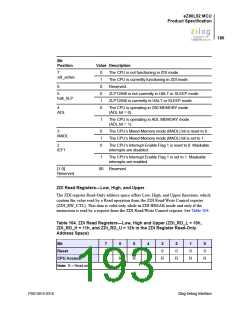
ZDI Write Memory Register
A Write to the ZDI Write Memory register causes the ZLP12840 to write the 8-bit data to
the memory location specified by the current address in the program counter. In Z80
MEMORY mode, this address is {MBASE, PC[15:0]}. In ADL MEMORY mode, this
address is PC[23:0]. The program counter, PC, increments after each data Write. However,
the ZDI register address does not increment automatically when this register is accessed.
As a result, the ZDI master is allowed to write any number of data bytes by writing to this
address one time followed by any number of data bytes. See Table 99.
Table 99. ZDI Write Memory Register (ZDI_WR_MEM = 30h in the ZDI
Register Write-Only Address Space)
Bit
7
X
6
X
5
X
4
X
3
X
2
X
1
X
0
X
Reset
CPU Access
W
W
W
W
W
W
W
W
Note: X = Undefined; W = Write.
PS013015-0316
Zilog Debug Interface

 ZILOG [ ZILOG, INC. ]