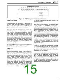
Initialisation MT312
e.g. For a crystal frequency of 10MHz, a system
clock frequency of 60MHz, the PLL ratio will be 6,
requiring the PLL FACTOR[1:0] = 2.
3 MT312 Initialisation
3.1 The Configuration Register (127)
For QPSK reception and ADC internal, the MT312 is
enabled by writing 88 hex to register 127.
CONFIG[B7-0]: This register is for setting up the
MT312. It must be loaded first before any other
register. It can only be reset to the default value by
the RESET pin being pulled low. After loading this
register, wait 150µs for the Clock PLL to settle before
writing to the RESET register. During this wait
period, the tuner may be programmed via the
General Purpose Port. Note that the GPP register
occupies the address space before the RESET
register.
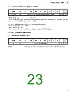
MT312 computes the System clock frequency using
bits B3-B1 above. This frequency is used internally
for computing parameters needed for acquiring the
QPSK signal.
It is possible to use a crystal frequency other than 10
or 15 MHz. As an example, let the crystal frequency
be 10.25MHz and the PLL multiplication factor be 6.
Then B3 is set to 1 and B2 to 0. Bit B1 may be given
an arbitrary value (0 or 1). The external software
must compute the system clock frequency and load
this value (multiplied by 2) to the SYS CLK register
(Address 34). In the above example, the system
clock frequency is 61.5 MHz and hence the value
123 has to be loaded into SYS CLK register.
CONFIG[B7]: 312 ENHigh = MT312 enable.
Low = MT312 disable to save power.
CONFIG[B6-5]: DSS BDSS A
0
0
1
1
0: DVB mode
1: DSS mode 1 - code rate 2/3
0: DSS mode 2 - code rate 6/7
1: DSS Code Rate search
The QPSK demodulator checks the SYS CLK
register and if this is non-zero, it uses the contents of
this as the system clock frequency, for internal
calculations mentioned above. If this register is zero
(which is the default setting), QPSK demodulator
works out the system clock frequency from bits B3-
B1 of the CONFIG register assuming that the crystal
frequency is either 10 or 15 MHz, as defined by bit
B1.
If both DSS A and DSS B are set high, the MT312
will search for the code rate in DSS mode. If either of
the DSS A or DSS B are set high, the Symbol rate is
automatically set to 20Mbaud and SYM RATE
registers (23 & 24) are ignored. The matched filter
root-raised-cosine roll-off is set to 0.20 and bit B0 of
QPSK CTRL (26) is ignored. Also, any code rate
programmed into VIT MODE register (25) and VIT
SETUP register (86) will be ignored.
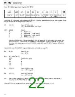
3.2 Power Supplies
To avoid the possibility of destructive latch-up, the
CVDD supply must never, at any time during power-
up, exceed 0·5V above the VDD supply and must
also remain within the absolute maximum ratings,
see section 12.2 on page 78.
Also in DSS mode TS SW RATE register (50) must
be set to 20, see 10.2.10 Timing Synchronisation
Sweep Rate. Register 50 (R/W).
VDD
CONFIG[B4]: BPSK High = BPSK
Low = QPSK
CVDD
RESET
CONFIG[B3-2]: PLL FACTOR[1:0]:
B3-2 Multiplication factor
00:
01:
10:
11:
3
4
6
9
Don’t care
~1ms typ.
Don’t care
ADDR[7:1]
SLEEP
Osc
CONFIG[B1]: CRYS15 High = 15MHz crystal.
Low = 10MHz crystal.
Figure 14 - MT351 power-up sequence
CONFIG[B0]: ADCEXT High = ADC external.
Low = ADC internal.
In general therefore, the VDD supply should be
established ahead of, or simultaneously with the
C
supply.
VDD
19

 ZARLINK [ ZARLINK SEMICONDUCTOR INC ]