MA28138
A single ‘Proceed’ instruction sent by the CTU addressed
to the TA of the ‘talker’ causes one data word to be transferred
if either the I- or R-bus has been selected and a contiguous
block of data words to be transferred if the BT-bus has been
selected.
Address and no commands are permitted at the Broadcast
Address). This strategy does not, however, permit the CTU to
perform operations such as the simultaneous set-up of a group
of connected RBls or the broadcast of blocks of data to all RBls
without explicitly addressing each RBI in turn.
Facilities for conducting broadcast RBI setup and CTU-RBI
transfers using the all-‘1’s BroadCast Address (BC) are also
available when the Extended Addressing mode is enabled by
setting the EXTAEN pin to ‘1’.
The MA28138 instruction decoder is designed so that by
setting the EXTAEN (Extended Addressing Enable) pin to ‘1’,
all commands which may be physically performed by a
network of RBI devices without electrical hazard are permitted
using either the Programmed Address or the Broadcast
Address. The only restrictions on permissible commands in
this mode are those caused by the need to have only one bus
‘talker’ on the network. Note, however, that in this mode, no
response is generated by any ‘listening’ RBI device addressed
using its PA. (One method here is to set the group’s PA to be
the same as the TA of the ‘talker’). It will be necessary to check
that each RBI in the group has been correctly set up or that
transferred blocks of data have been successfully received, for
example by asking each listener in turn for its status and/or
next DMA address or to return a software-generated
checksum.
For full compliance with the ESA RBI-2 WDI/CS/928
protocol, EXTAEN should be set to ‘0’. Full detatils of which
commands are accepted under the Basic Addressing mode
(EXTAEN = ‘0’) and the Extended Addressing mode (EXTAEN
= ‘1’) are given in Table 2. Note that the Programmed Address
(PA) within the MA28138 can not be programmed (in any way)
by using commands directed to either the Programmed
Address or the Broadcast Address. Setting the Programmed
Address to a 5-bit or 6-bit all-‘1’s field (depending on the
terminal address format in use) causes it to be considered as
invalid.
6. CONFIGURATION
The Broadcast Pulse outputs, User Control Command
outputs and Bi-Level Status inputs can be configured to
specific mission requirements.
7. TERMINAL ADDRESSING
Both standard (5 bit) and extended (6 bit) terminal
addressing formats are provided. Setting the EXTFMT
(Extended terminal address Format) pin to ‘0’ causes standard
(5 bit) terminal addressing to be used, Interrogation bit 6 to be
regarded as BCP(4) and the hard-wired TA(0) (MSB) input to
be ignored. Setting EXTFMT to ‘1’ causes extended (6 bit)
addressing to be used, Interrogation bit 6 to be regarded as
TA(0) (MSB) and BCP(4) output to be forced to ‘0’.
8. ADDRESSING MODES
ESA specify the availability of each command in the RBI-2
protocol instruction set when addressing is performed at the
hard-wired Terminal Address, the Programmable Address and
the (all-‘1’s) Broadcast Address. The RBI-2 protocol only
permits the use of a minimal set of commands which are
needed to achieve the transport of data blocks (specifically
only ‘Proceed’ commands are permitted at the Programmed
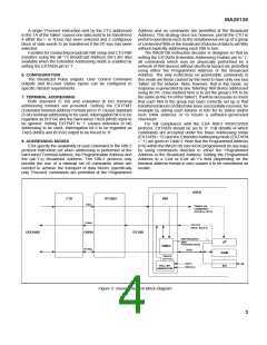
USER
CTU
RT-DBU
RBI
I-Bus
TIMING and
COMMANDS
UCC(0:6), UCCS
R-Bus
STATUS
SREQ, BIL(0:5)
GROUND
OBDH
RT-DBI
DMA REQUEST
DMA
ACKNOWLEDGE
µP
DMAC
BT-Bus
DATA
RAM
SINGLE
BIT POLL
GI(0:1)
POLL BIT
GENERATOR
I/O
PBP(0:4)
Figure 3: General System Block Diagram
3

 ZARLINK [ ZARLINK SEMICONDUCTOR INC ]