L9216B/H
Preliminary Data Sheet
September 2001
High-Voltage Ringing SLIC with Ground Start
Supervision (continued)
Power Ring (continued)
Sine Wave Input Signal and Sine Wave Power Ring Signal Output (continued)
During nonring modes, the sinusoidal ringing waveform may be left on at RINGIN. Via the state table, the ring signal
will be removed from tip and ring even if the low-voltage input is still present at RINGIN. There are certain timing
considerations that should be made with respect to state changes which are detailed in the Switching Behavior of
L9215/6 Ringing SLIC Application Note.
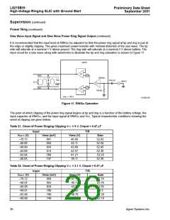
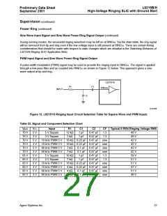
PWM Input Signal and Sine Wave Power Ring Signal Output
A pulse-width modulated (PWM) signal may be used to provide the ringing input to RINGIN. The signal is applied
through a low-pass filter and ac-coupled into RINGIN as shown in Figure 12 below. This approach gives a sine
wave output at tip and ring.
L9215/16
R1
C2
RINGIN
INPUT
C1
12-3578bF
Figure 12. L9215/16 Ringing Input Circuit Selection Table for Square Wave and PWM Inputs
Table 23. Signal and Component Selection Chart
VBAT
70 V
70 V
70 V
70 V
70 V
70 V
85 V
85 V
85 V
85 V
85 V
85 V
VCC
5 V
3 V
5 V
3 V
5 V
3 V
5 V
3 V
5 V
3 V
5 V
3 V
Input
R1
C1
C2
CF Typical 5 REN Ringing Voltage RMS
5 V Square
3 V Square
12 kΩ
7 kΩ
1 µF
1 µF
0.47 µF
0.47 µF
1.3
1.3
48 V
49 V
42 V
42 V
42 V
42 V
59 V
51 V
51 V
47 V
51 V
49 V
10 kHz PWM 5 V 10 kΩ 0.22 µF 0.47 µF sine
10 kHz PWM 3 V 10 kΩ 0.22 µF 0.47 µF sine
90 kHz PWM 5 V
90 kHz PWM 3 V
5 V Square
7 kΩ
7 kΩ
0.1 µF 0.47 µF sine
0.1 µF 0.47 µF sine
10 kΩ
7 kΩ
1 µF
1 µF
0.47 µF
0.47 µF
1.3
1.3
3 V Square
10 kHz PWM 5 V 10 kΩ 0.22 µF 0.47 µF sine
10 kHz PWM 3 V
90 kHz PWM 5 V
90 kHz PWM 3 V
4 kΩ 0.22 µF 0.47 µF sine
4 kΩ
4 kΩ
0.1 µF 0.47 µF sine
0.1 µF 0.47 µF sine
Agere Systems Inc.
27

 ZARLINK [ ZARLINK SEMICONDUCTOR INC ]